 | –≠–ª–µ–∫—Ç—Ä–æ–Ω–Ω—ã–π –∫–æ–º–ø–æ–Ω–µ–Ω—Ç: LAN83C183 | –°–∫–∞—á–∞—Ç—å:  PDF PDF  ZIP ZIP |

SMSC DS ≠ LAN83C183
Rev. 12/14/2000
LAN83C183
PRELIMINARY
10/100 Mbps TX/FX/10BT
Fast Ethernet Physical Layer Device (PHY)
Features
∑
Single-Chip 100BASE-TX/FX/10BASE-T Fast
Ethernet Physical Layer Solution
∑
Dual-Speed - 10/100 Mbits/sec
∑
Half-Duplex And Full-Duplex Support
∑
MII Interface to Ethernet Controller
∑
MI Interface for Configuration and Status
∑
Optional Repeater Interface
∑
AutoNegotiation: 10/100, Full/Half-Duplex
∑
Meets All Applicable IEEE 802.3 Standards
∑
On-Chip Wave Shaping - No External Filters
Required
∑
Adaptive Equalizer
∑
Baseline Wander Correction
∑
Interface to External 100BASE-T4 PHY
∑
LED Outputs
≠
Link
≠
Activity
≠
Collision
≠
Full Duplex
≠
10/100
≠
User-Programmable
∑
Many User Features and Options
∑
Few External Components
∑
3.3V Supply with 5V-Tolerant I/O
∑
64-Pin TQFP Package (1.4-mm Body
Thickness)
GENERAL DESCRIPTION
The SMSC LAN83C183 is a highly integrated analog interface IC for twisted pair Ethernet applications.
The LAN83C183 can be configured for either 100-Mbps (100BASE-TX or 100 BASE-FX) or 10-Mbps
(10BASE-T) Ethernet operation. The 100BASE-FX is packaged in a 64-Pin TQFP pack-age.
The LAN83C183 consists of a 4B5B/Manchester encoder/decoder, scrambler/descrambler, transmitter
with wave shaping and output driver, twisted pair receiver with on-chip equalizer and baseline wander
correction, clock and data recovery, AutoNegotiation, controller interface (MII), and serial port (MI).
The addition of internal output waveshaping circuitry and on-chip filters eliminates the need for external
filters normally required in 100BASE-TX and 10BASE-T applications.
The LAN83C183 can automatically configure itself for 100- or 10-Mbps and full- or half-duplex operation
with the on-chip AutoNegotiation algorithm.
The eleven 16-bit registers of the LAN83C183 can be accessed through the Management Interface (MI)
serial port. These registers contain configuration inputs, status outputs, and device capabilities.
The LAN83C183 is ideal as a media interface for 100BASE-TX/10BASE-T adapter cards, PC Cards,
motherboards, mobile applications, repeaters, switching hubs, and external PHYs.
The LAN83C183 operates from a single 3.3V supply. All inputs and outputs are 5V-tolerant and can
directly interface to other 5V devices.

SMSC DS ≠ LAN83C183
2
Rev. 12/14/2000
© STANDARD MICROSYSTEMS CORPORATION (SMSC) 2000
80 Arkay Drive
Hauppauge, NY 11788
(631) 435-6000
FAX (631) 273-3123
Standard Microsystems is a registered trademark of Standard Microsystems Corporation, and SMSC is a trademark of Standard
Microsystems Corporation. Pentium is a registered trademark of Intel Corporation. Product names and company names are the
trademarks of their respective holders. Circuit diagrams utilizing SMSC products are included as a means of illustrating typical
applications; consequently complete information sufficient for construction purposes is not necessarily given. Although the
information has been checked and is believed to be accurate, no responsibility is assumed for inaccuracies. SMSC reserves the
right to make changes to specifications and product descriptions at any time without notice. Contact your local SMSC sales office
to obtain the latest specifications before placing your product order. The provision of this information does not convey to the
purchaser of the semiconductor devices described any licenses under the patent rights of SMSC or others. All sales are expressly
conditional on your agreement to the terms and conditions of the most recently dated version of SMSC's standard Terms of Sale
Agreement dated before the date of your order (the "Terms of Sale Agreement"). The product may contain design defects or errors
known as anomalies which may cause the product's functions to deviate from published specifications. Anomaly sheets are
available upon request. SMSC products are not designed, intended, authorized or warranted for use in any life support or other
application where product failure could cause or contribute to personal injury or severe property damage. Any and all such uses
without prior written approval of an Officer of SMSC and further testing and/or modification will be fully at the risk of the customer.
Copies of this document or other SMSC literature, as well as the Terms of Sale Agreement, may be obtained by visiting SMSC's
website at http://www.smsc.com.
SMSC DISCLAIMS AND EXCLUDES ANY AND ALL WARRANTIES, INCLUDING WITHOUT LIMITATION ANY AND ALL IMPLIED
WARRANTIES OF MERCHANTABILITY, FITNESS FOR A PARTICULAR PURPOSE, TITLE, AND AGAINST INFRINGEMENT,
AND ANY AND ALL WARRANTIES ARISING FROM ANY COURSE OF DEALING OR USAGE OF TRADE.
IN NO EVENT SHALL SMSC BE LIABLE FOR ANY DIRECT, INCIDENTAL, INDIRECT, SPECIAL, PUNITIVE, OR
CONSEQUENTIAL DAMAGES, OR FOR LOST DATA, PROFITS, SAVINGS OR REVENUES OF ANY KIND; REGARDLESS OF
THE FORM OF ACTION, WHETHER BASED ON CONTRACT, TORT, NEGLIGENCE OF SMSC OR OTHERS, STRICT LIABILITY,
BREACH OF WARRANTY, OR OTHERWISE; WHETHER OR NOT ANY REMEDY IS HELD TO HAVE FAILED OF ITS ESSENTIAL
PURPOSE; AND WHETHER OR NOT SMSC HAS BEEN ADVISED OF THE POSSIBILITY OF SUCH DAMAGES.
ORDERING INFORMATION
Order Number:
LAN83C183-JD
64-Pin TQFP Package

SMSC DS ≠ LAN83C183
3
Rev. 12/14/2000
Contents
Chapter 1
LAN83C183 Functional Description
1.1
OVERVIEW . . . . . . . . . . . . . . . . . . . . . . . . . . . . . . . . . . . . . . . . . . . . . . . . . . 11
1.1.1
Channel Operation . . . . . . . . . . . . . . . . . . . . . . . . . . . . . . . . . . . . . 11
1.1.2
Data Paths . . . . . . . . . . . . . . . . . . . . . . . . . . . . . . . . . . . . . . . . . . . 11
1.2
BLOCK DIAGRAM DESCRIPTION . . . . . . . . . . . . . . . . . . . . . . . . . . . . . . . . 16
1.2.1
Oscillator and Clock . . . . . . . . . . . . . . . . . . . . . . . . . . . . . . . . . . . . 16
1.2.2
Controller Interface . . . . . . . . . . . . . . . . . . . . . . . . . . . . . . . . . . . . . 16
1.2.3
Encoder . . . . . . . . . . . . . . . . . . . . . . . . . . . . . . . . . . . . . . . . . . . . . . 20
1.2.4
Decoder. . . . . . . . . . . . . . . . . . . . . . . . . . . . . . . . . . . . . . . . . . . . . . 22
1.2.5
Scrambler . . . . . . . . . . . . . . . . . . . . . . . . . . . . . . . . . . . . . . . . . . . . 23
1.2.6
Descrambler . . . . . . . . . . . . . . . . . . . . . . . . . . . . . . . . . . . . . . . . . . 23
1.2.7
Twisted-Pair Transmitters . . . . . . . . . . . . . . . . . . . . . . . . . . . . . . . . 24
1.2.8
Twisted-Pair Receivers . . . . . . . . . . . . . . . . . . . . . . . . . . . . . . . . . . 27
1.2.9
FX Transmitter and Receiver . . . . . . . . . . . . . . . . . . . . . . . . . . . . . 29
1.2.10
Clock and Data Recovery. . . . . . . . . . . . . . . . . . . . . . . . . . . . . . . . 31
1.2.11
Link Integrity and AutoNegotiation . . . . . . . . . . . . . . . . . . . . . . . . . 31
1.2.12
Link Indication . . . . . . . . . . . . . . . . . . . . . . . . . . . . . . . . . . . . . . . . . 34
1.2.13
Collision. . . . . . . . . . . . . . . . . . . . . . . . . . . . . . . . . . . . . . . . . . . . . . 35
1.2.14
LED Drivers. . . . . . . . . . . . . . . . . . . . . . . . . . . . . . . . . . . . . . . . . . . 36
1.3
START OF PACKET . . . . . . . . . . . . . . . . . . . . . . . . . . . . . . . . . . . . . . . . . . . 38
1.3.1
100 Mbits/s . . . . . . . . . . . . . . . . . . . . . . . . . . . . . . . . . . . . . . . . . . . 38
1.3.2
10 Mbits/s . . . . . . . . . . . . . . . . . . . . . . . . . . . . . . . . . . . . . . . . . . . . 38
1.4
END OF PACKET . . . . . . . . . . . . . . . . . . . . . . . . . . . . . . . . . . . . . . . . . . . . . 39
1.4.1
100 Mbits/s . . . . . . . . . . . . . . . . . . . . . . . . . . . . . . . . . . . . . . . . . . . 39
1.4.2
10 Mbits/s . . . . . . . . . . . . . . . . . . . . . . . . . . . . . . . . . . . . . . . . . . . . 39
1.5
FULL/HALF DUPLEX MODE. . . . . . . . . . . . . . . . . . . . . . . . . . . . . . . . . . . . . 41
1.5.1
Forcing Full/Half Duplex Operation . . . . . . . . . . . . . . . . . . . . . . . . 41
1.5.2
Full/Half Duplex Indication . . . . . . . . . . . . . . . . . . . . . . . . . . . . . . . 41
1.5.3
Loopback. . . . . . . . . . . . . . . . . . . . . . . . . . . . . . . . . . . . . . . . . . . . . 41
1.6
REPEATER MODE . . . . . . . . . . . . . . . . . . . . . . . . . . . . . . . . . . . . . . . . . . . . 42
1.7
10/100 MBITS/S SELECTION . . . . . . . . . . . . . . . . . . . . . . . . . . . . . . . . . . . . 42
1.7.1
Forcing 10/100 Mbits/s Operation . . . . . . . . . . . . . . . . . . . . . . . . . 42
1.7.2
Autoselecting 10/100 Mbits/s Operation. . . . . . . . . . . . . . . . . . . . . 42
1.7.3
10/100 Mbits/s Indication . . . . . . . . . . . . . . . . . . . . . . . . . . . . . . . . 42
1.8
JABBER . . . . . . . . . . . . . . . . . . . . . . . . . . . . . . . . . . . . . . . . . . . . . . . . . . . . . 43

SMSC DS ≠ LAN83C183
4
Rev. 12/14/2000
1.9
AUTOMATIC JAM . . . . . . . . . . . . . . . . . . . . . . . . . . . . . . . . . . . . . . . . . . . . . 43
1.9.1
100 Mbits/s JAM . . . . . . . . . . . . . . . . . . . . . . . . . . . . . . . . . . . . . . . 43
1.9.2
10 Mbits/s JAM . . . . . . . . . . . . . . . . . . . . . . . . . . . . . . . . . . . . . . . . 43
1.10
RESET . . . . . . . . . . . . . . . . . . . . . . . . . . . . . . . . . . . . . . . . . . . . . . . . . . . . . . 44
1.11
POWERDOWN . . . . . . . . . . . . . . . . . . . . . . . . . . . . . . . . . . . . . . . . . . . . . . . 44
1.12
RECEIVE POLARITY CORRECTION . . . . . . . . . . . . . . . . . . . . . . . . . . . . . . 44
Chapter 2
Signal Descriptions
2.1
MEDIA INTERFACE SIGNALS . . . . . . . . . . . . . . . . . . . . . . . . . . . . . . . . . . . 46
2.2
CONTROLLER INTERFACE SIGNALS (MII) . . . . . . . . . . . . . . . . . . . . . . . . 47
2.3
MANAGEMENT INTERFACE . . . . . . . . . . . . . . . . . . . . . . . . . . . . . . . . . . . . 48
2.4
MISCELLANEOUS SIGNALS . . . . . . . . . . . . . . . . . . . . . . . . . . . . . . . . . . . . 48
2.5
LEDS . . . . . . . . . . . . . . . . . . . . . . . . . . . . . . . . . . . . . . . . . . . . . . . . . . . . . . . 50
2.6
POWER SUPPLY . . . . . . . . . . . . . . . . . . . . . . . . . . . . . . . . . . . . . . . . . . . . . 51
Chapter 3
Registers
3.1
BIT TYPES . . . . . . . . . . . . . . . . . . . . . . . . . . . . . . . . . . . . . . . . . . . . . . . . . . . 54
3.2
MI SERIAL PORT REGISTER SUMMARY. . . . . . . . . . . . . . . . . . . . . . . . . . 55
3.3
REGISTERS. . . . . . . . . . . . . . . . . . . . . . . . . . . . . . . . . . . . . . . . . . . . . . . . . . 57
3.3.1
Control Register (Register 0) . . . . . . . . . . . . . . . . . . . . . . . . . . . . . 57
3.3.2
Status Register (Register 1) . . . . . . . . . . . . . . . . . . . . . . . . . . . . . . 58
3.3.3
PHY ID 1 Register (Register 2) . . . . . . . . . . . . . . . . . . . . . . . . . . . 60
3.3.4
PHY ID 2 Register (Register 3) . . . . . . . . . . . . . . . . . . . . . . . . . . . 61
3.3.5
AutoNegotiation Advertisement Register (Register 4) . . . . . . . . . . 61
3.3.6
AutoNegotiation Remote End Capability Register (Register 5) . . . 63
3.3.7
Configuration 1 Register (Register 16). . . . . . . . . . . . . . . . . . . . . . 64
3.3.8
Configuration 2 Register (Register 17). . . . . . . . . . . . . . . . . . . . . . 66
3.3.9
Status Output Register (Register 18) . . . . . . . . . . . . . . . . . . . . . . . 68
3.3.10
Interrupt Mask Register (Register 19) . . . . . . . . . . . . . . . . . . . . . . 69
3.3.11
Reserved Register (Register 20) . . . . . . . . . . . . . . . . . . . . . . . . . . 71
Chapter 4
Management Interface
4.1
SIGNAL DESCRIPTION . . . . . . . . . . . . . . . . . . . . . . . . . . . . . . . . . . . . . . . . 74
4.2
GENERAL OPERATION . . . . . . . . . . . . . . . . . . . . . . . . . . . . . . . . . . . . . . . . 75
4.3
MULTIPLE REGISTER ACCESS . . . . . . . . . . . . . . . . . . . . . . . . . . . . . . . . . 75
4.4
FRAME STRUCTURE . . . . . . . . . . . . . . . . . . . . . . . . . . . . . . . . . . . . . . . . . . 77
4.5
REGISTER STRUCTURE . . . . . . . . . . . . . . . . . . . . . . . . . . . . . . . . . . . . . . . 78
4.6
INTERRUPTS . . . . . . . . . . . . . . . . . . . . . . . . . . . . . . . . . . . . . . . . . . . . . . . . 79
Chapter 5
Specifications
5.1
ABSOLUTE MAXIMUM RATINGS . . . . . . . . . . . . . . . . . . . . . . . . . . . . . . . . 82
5.2
ELECTRICAL CHARACTERISTICS . . . . . . . . . . . . . . . . . . . . . . . . . . . . . . . 83
5.2.1
Twisted-Pair DC Characteristics . . . . . . . . . . . . . . . . . . . . . . . . . . . 84
5.2.2
FX Characteristics, Transmit . . . . . . . . . . . . . . . . . . . . . . . . . . . . . 87
5.3
AC ELECTRICAL CHARACTERISTICS . . . . . . . . . . . . . . . . . . . . . . . . . . . . 89
5.3.1
25 MHz Input/Output Clock Timing Characteristics . . . . . . . . . . . . 90

SMSC DS ≠ LAN83C183
5
Rev. 12/14/2000
5.3.2
Transmit Timing Characteristics . . . . . . . . . . . . . . . . . . . . . . . . . . . 91
5.3.3
Receive Timing Characteristics . . . . . . . . . . . . . . . . . . . . . . . . . . . 93
5.3.4
Collision and JAM Timing Characteristics . . . . . . . . . . . . . . . . . . . 97
5.3.5
Link Pulse Timing Characteristics . . . . . . . . . . . . . . . . . . . . . . . . 100
5.3.6
Jabber Timing Characteristics . . . . . . . . . . . . . . . . . . . . . . . . . . . 103
5.4
LED DRIVER TIMING CHARACTERISTICS . . . . . . . . . . . . . . . . . . . . . . . 104
5.4.1
MI Serial Port Timing Characteristics . . . . . . . . . . . . . . . . . . . . . . 105
5.5
PINOUTS AND PACKAGE DRAWINGS. . . . . . . . . . . . . . . . . . . . . . . . . . . 107
5.5.1
Pinouts . . . . . . . . . . . . . . . . . . . . . . . . . . . . . . . . . . . . . . . . . . . . . 107
5.5.2
LAN83C183 Pin Layout . . . . . . . . . . . . . . . . . . . . . . . . . . . . . . . . 112
5.6
MECHANICAL DRAWING . . . . . . . . . . . . . . . . . . . . . . . . . . . . . . . . . . . . . . 113

SMSC DS ≠ LAN83C183
6
Rev. 12/14/2000

SMSC DS ≠ LAN83C183
7
Rev. 12/14/2000
Figures
1.1
LAN83C183 Device Block Diagram . . . . . . . . . . . . . . . . . . . . . . . . . . . . . . . 12
1.2
100BASE-TX/FX and 10BASE-T Frame Format . . . . . . . . . . . . . . . . . . . . . 13
1.3
MII Frame Format . . . . . . . . . . . . . . . . . . . . . . . . . . . . . . . . . . . . . . . . . . . . . 14
1.4
TP Output Voltage Template . . . . . . . . . . . . . . . . . . . . . . . . . . . . . . . . . . . . 25
1.5
TP Input Voltage Template (10 Mbits/s) . . . . . . . . . . . . . . . . . . . . . . . . . . . . 28
1.6
Link Pulse Output Voltage Template (10 Mbits/s) . . . . . . . . . . . . . . . . . . . . 32
1.7
NLP vs FLP Link Pulse . . . . . . . . . . . . . . . . . . . . . . . . . . . . . . . . . . . . . . . . 33
1.8
SOI Output Voltage Template - 10 Mbits/s . . . . . . . . . . . . . . . . . . . . . . . . . 40
2.1
Device Logic Diagram. . . . . . . . . . . . . . . . . . . . . . . . . . . . . . . . . . . . . . . . . . 45
4.1
MI Serial Port Frame Timing Diagram . . . . . . . . . . . . . . . . . . . . . . . . . . . . . 75
4.2
MI Serial Frame Structure . . . . . . . . . . . . . . . . . . . . . . . . . . . . . . . . . . . . . . 77
4.3
MDIO Interrupt Pulse . . . . . . . . . . . . . . . . . . . . . . . . . . . . . . . . . . . . . . . . . . 79
5.1
25 MHz Output Timing . . . . . . . . . . . . . . . . . . . . . . . . . . . . . . . . . . . . . . . . . 90
5.2
Transmit Timing - 100 Mbits/s . . . . . . . . . . . . . . . . . . . . . . . . . . . . . . . . . . . 92
5.3
Transmit Timing - 10 Mbits/s . . . . . . . . . . . . . . . . . . . . . . . . . . . . . . . . . . . . 92
5.4
Receive Timing, Start of Packet - 100 Mbits/s . . . . . . . . . . . . . . . . . . . . . . 94
5.5
Receive Timing, End of Packet - 100 Mbits/s . . . . . . . . . . . . . . . . . . . . . . . 95
5.6
Receive Timing, Start of Packet - 10 Mbits/s . . . . . . . . . . . . . . . . . . . . . . . 95
5.7
Receive Timing, End of Packet - 10 Mbits/s . . . . . . . . . . . . . . . . . . . . . . . . 96
5.8
RX_EN Timing . . . . . . . . . . . . . . . . . . . . . . . . . . . . . . . . . . . . . . . . . . . . . . . 96
5.9
Collision Timing, Receive 100 Mbits/s . . . . . . . . . . . . . . . . . . . . . . . . . . . . . 97
5.10
Collision Timing, Receive 10 Mbits/s . . . . . . . . . . . . . . . . . . . . . . . . . . . . . . 98
5.11
Collision Timing, Transmit - 100 Mbits/s . . . . . . . . . . . . . . . . . . . . . . . . . . . 98
5.12
Collision Timing, Transmit - 10 Mbits/s . . . . . . . . . . . . . . . . . . . . . . . . . . . . 98
5.13
Collision Test Timing . . . . . . . . . . . . . . . . . . . . . . . . . . . . . . . . . . . . . . . . . . . 99
5.14
JAM Timing . . . . . . . . . . . . . . . . . . . . . . . . . . . . . . . . . . . . . . . . . . . . . . . . . . 99
5.15
NLP Link Pulse Timing . . . . . . . . . . . . . . . . . . . . . . . . . . . . . . . . . . . . . . . . 101
5.16
FLP Link Pulse Timing . . . . . . . . . . . . . . . . . . . . . . . . . . . . . . . . . . . . . . . . 102
5.17
Jabber Timing . . . . . . . . . . . . . . . . . . . . . . . . . . . . . . . . . . . . . . . . . . . . . . . 103
5.18
LED Driver Timing . . . . . . . . . . . . . . . . . . . . . . . . . . . . . . . . . . . . . . . . . . . 104
5.19
MI Serial Port Timing . . . . . . . . . . . . . . . . . . . . . . . . . . . . . . . . . . . . . . . . . 105
5.20
MDIO Interrupt Pulse Timing . . . . . . . . . . . . . . . . . . . . . . . . . . . . . . . . . . . 106
5.21
LAN83C183 64-Pin LQFP, Top View . . . . . . . . . . . . . . . . . . . . . . . . . . . . . 112
5.22
64-Pin LQFP Mechanical Drawing . . . . . . . . . . . . . . . . . . . . . . . . . . . . . . . 113

SMSC DS ≠ LAN83C183
8
Rev. 12/14/2000

SMSC DS ≠ LAN83C183
9
Rev. 12/14/2000
Tables
1.1
Transmit Preamble and SFD Bits at MAC Nibble Interface . . . . . . . . . . . . 14
1.2
Receive Preamble and SFD Bits at MAC Nibble Interface . . . . . . . . . . . . . 15
1.3
4B/5B Symbol Mapping . . . . . . . . . . . . . . . . . . . . . . . . . . . . . . . . . . . . . . . . 18
1.4
4B/5B Symbol Mapping . . . . . . . . . . . . . . . . . . . . . . . . . . . . . . . . . . . . . . . . 21
1.5
TP Output Voltage - 10 Mbits/s . . . . . . . . . . . . . . . . . . . . . . . . . . . . . . . . . . 25
1.6
Transmit Level Adjust . . . . . . . . . . . . . . . . . . . . . . . . . . . . . . . . . . . . . . . . . . 26
1.7
FX Transmit Level Adjust . . . . . . . . . . . . . . . . . . . . . . . . . . . . . . . . . . . . . . . 30
1.8
PLED_[1:0] Output Select Bit Encoding. . . . . . . . . . . . . . . . . . . . . . . . . . . . 36
1.9
LED Normal Function Definition . . . . . . . . . . . . . . . . . . . . . . . . . . . . . . . . . . 37
1.10
LED Event Definition. . . . . . . . . . . . . . . . . . . . . . . . . . . . . . . . . . . . . . . . . . . 37
3.1
MI Register Bit Type Definition . . . . . . . . . . . . . . . . . . . . . . . . . . . . . . . . . . 54
4.1
MI Serial Port Register Summary. . . . . . . . . . . . . . . . . . . . . . . . . . . . . . . . . 78
5.1
Absolute Maximum Ratings . . . . . . . . . . . . . . . . . . . . . . . . . . . . . . . . . . . . . 82
5.2
DC Characteristics . . . . . . . . . . . . . . . . . . . . . . . . . . . . . . . . . . . . . . . . . . . . 83
5.3
Twisted Pair Characteristics (Transmit ). . . . . . . . . . . . . . . . . . . . . . . . . . . . 84
5.4
Twisted Pair Characteristics (Receive ) . . . . . . . . . . . . . . . . . . . . . . . . . . . . 86
5.5
FX Characteristics, Transmit . . . . . . . . . . . . . . . . . . . . . . . . . . . . . . . . . . . . 87
5.6
FX Characteristics, Receive . . . . . . . . . . . . . . . . . . . . . . . . . . . . . . . . . . . . . 88
5.7
Test Conditions . . . . . . . . . . . . . . . . . . . . . . . . . . . . . . . . . . . . . . . . . . . . . . . 89
5.8
25 MHz Input/Output Clock . . . . . . . . . . . . . . . . . . . . . . . . . . . . . . . . . . . . . 90
5.9
Transmit Timing . . . . . . . . . . . . . . . . . . . . . . . . . . . . . . . . . . . . . . . . . . . . . 91
5.10
Receive Timing . . . . . . . . . . . . . . . . . . . . . . . . . . . . . . . . . . . . . . . . . . . . . . 93
5.11
Collision and Jam Timing . . . . . . . . . . . . . . . . . . . . . . . . . . . . . . . . . . . . . . 97
5.12
Link Pulse Timing . . . . . . . . . . . . . . . . . . . . . . . . . . . . . . . . . . . . . . . . . . . 100
5.13
Jabber Timing . . . . . . . . . . . . . . . . . . . . . . . . . . . . . . . . . . . . . . . . . . . . . . . 103
5.14
LED Driver Timing . . . . . . . . . . . . . . . . . . . . . . . . . . . . . . . . . . . . . . . . . . . 104
5.15
MI Serial Port Timing . . . . . . . . . . . . . . . . . . . . . . . . . . . . . . . . . . . . . . . . . 105
5.16
LAN83C183 Pin List (by Signal Category) . . . . . . . . . . . . . . . . . . . . . . . . 107
5.17
LAN83C183 Pin List (by Pin Number) . . . . . . . . . . . . . . . . . . . . . . . . . . . 110

SMSC DS ≠ LAN83C183
10
Rev. 12/14/2000

SMSC DS ≠ LAN83C183
11
Rev. 12/14/2000
Chapter 1
LAN83C183
Functional Description
This chapter is a functional description of the PHY device with the following sections:
∑
Section 1.1, "Overview"
∑
Section 1.2, "Block Diagram Description"
∑
Section 1.3, "Start of Packet"
∑
Section 1.4, "End of Packet"
∑
Section 1.5, "Full/Half Duplex Mode"
∑
Section 1.6, "Repeater Mode"
∑
Section 1.7, "10/100 Mbits/s Selection"
∑
Section 1.8, "Jabber"
∑
Section 1.9, "Automatic Jam"
∑
Section 1.10, "Reset"
∑
Section 1.11, "Powerdown"
∑
Section 1.12, "Receive Polarity Correction"
1.1 OVERVIEW
This section gives a brief overview of the device functional operation. The
LAN83C183 is a complete 10/100 Mbits/s Ethernet Media Interface IC. A block
diagram is shown in
Figure 1.1
.
1.1.1 Channel Operation
The PHY operates in the 100BASE-TX or 100BASE-FX modes at 100 Mbits/s, or in
the 10BASE-T mode at 10 Mbits/s. The 100 Mbits/s modes and the 10 Mbits/s mode
differ in data rate, signaling protocol, and allowed wiring as follows:
∑
100BASE-TX mode uses two pairs of category 5 or better UTP or STP twisted-
pair cable with 4B5B encoded, scrambled, and MLT3 coded 62.5-MHz ternary
data to achieve a throughput of 100 Mbits/s.
∑
The 100BASE-FX mode uses two fiber cables with 4B5B encoded, 125-MHz
binary data to achieve a throughput of 100 Mbits/s.
∑
10 Mbits/s mode uses two pairs of category 3 or better UTP or STP twisted-pair
cable with Manchester encoded 10-MHz binary data to achieve a 10 Mbits/s
throughput
The data symbol format on the twisted-pair cable for the 100 and 10 Mbits/s modes
is defined in IEEE 802.3 specifications and shown in
Figure 1.2
.
1.1.2 Data Paths
In each device, there is a transmit data path and a receive data path associated with
each PHY channel. The transmit data path is from the Controller Interface to the
twisted-pair transmitter. The receive data path is from the twisted-pair receiver to the
Controller Interface.
S
M
S
C
D
S
≠
L
A
N
8
3
C
1
8
3
1
2
R
e
v
.
1
2
/
1
4
/
2
0
0
0
Figure 1.1 LAN83C183 Device Block Diagram
Clock
Generator
PLL
OSCIN
RESETn
RX_EN/JAMn
RPTR
Interface
TX_CLK
TXD[3:0]
MDC
MDIO
Serial
Controller
TX_EN
TX_ER/TXD4
RX_CLK
RXD[3:0]
CRS
RX_DV
RX_ER/RXD4
Collision
4B5B
Encoder
Scrambler
MLT3
Encoder
Switched
Clock
Generator
LP
Filter
100BASE-TX Transmitter
ROM
DAC
LP
Filter
+
-
4B5B
Decoder
Descrambler
Clock
Recovery
& Data
Auto-
& Link
Negotiation
Adaptive
Equalizer
LP
Filter
TPO
+/
FXI
-
TPO
-/
FXI
+
+
-
100BASE-TX Receiver
10BASE-TX Receiver
Recovery
Clock & Data
(Manchester
Decoder)
Manchester
Encoder
10BASE-T Receiver
Oscillator
COL
PLED[3:0]n
MDA[3:0]n
LED
Drivers
Port
(MI)
VDD[6:1]
GND[6:1]
Current
Sources
PLL
Squelch
+/-
Vth
+
-
+
+/-
Vth
+
-
+
Squelch
MLT3
Encoder
(MII
PLED[5:4]n
REXT
+
-
100BASE-FX Transmitter
+/-
Vth
+
-
+
100BASE-TX Receiver
+
-
Vth
SD_THR
SD/FXDISn
TPI
+/
FXO
-
TPI
-/
FXO
+
MDINTn/MDA4n
or
FBI)
SMSC DS ≠ LAN83C183
13
Rev. 12/14/2000
Figure 1.2 100BASE-TX/FX and 10BASE-T Frame Format
Interframe
Gap
PREAMBLE
SFD
DA
SA
LN
LLC Data
FCS
Interframe
Gap
Ethernet MAC Frame
SSD
DA
SA
LN
LLC DATA
FCS
100BASE-TX Data Symbols
IDLE
PREAMBLE
SFD
ESD
IDLE
IDLE =
SSD =
PREAMBLE =
SFD =
DA, SA, LN, LLC DATA, FCS =
ESD =
[ 1 1 1 1 ...]
[ 1 1 0 0 0 1 0 0 0 1 ]
[ 1 0 1 0 ...] 62 Bits Long
[ 1 1 ]
[ DATA ]
[ 0 1 1 0 1 0 0 1 1 1 ]
Before/After
4B5B Encoding,
Scrambling, and
MLT3 Coding
DA
SA
LN
LLC DATA
FCS
10BASE-T Data Symbols
IDLE
PREAMBLE
SFD
SOI
IDLE
IDLE =
PREAMBLE =
SFD =
DA, SA, LN, LLC DATA, FCS =
[ No Transitions ]
[ 1 1 ]
[ DATA ]
[ 1 1 ] With No MID Bit
SOI =
Transition
[ 1 0 1 0 ...] 62 Bits Long
Before/After
Manchester
Encoding
SSD
DA
SA
LN
LLC DATA
FCS
100BASE-FX Data Symbols
IDLE
PREAMBLE
SFD
ESD
IDLE
IDLE =
SSD =
PREAMBLE =
SFD =
DA, SA, LN, LLC DATA, FCS =
ESD =
[ 1 1 1 1 ...]
[ 1 1 0 0 0 1 0 0 0 1 ]
[ 1 0 1 0 ...] 62 Bits Long
[ 1 1 ]
[ DATA ]
[ 0 1 1 0 1 0 0 1 1 1 ]
Before/After
4B5B Encoding

SMSC DS ≠ LAN83C183
14
Rev. 12/14/2000
1.1.2.1 100BASE-TX
In 100BASE-TX transmit operation, data is received on the Controller Interface from
an external Ethernet controller in the format shown in
Figure 1.3
and
Table 1.1
. The
data is sent to the 4B5B encoder, which scrambles the encoded data. The scrambled
data is then sent to the TP transmitter. The TP transmitter converts the encoded and
scrambled data into MLT3 ternary format, preshapes the output, and drives the
twisted-pair cable.
Figure 1.3 MII Frame Format
In 100BASE-TX receive operation, the TP receiver takes incoming encoded and
scrambled MLT3 data from the twisted-pair cable, removes any high-frequency noise
from the input, equalizes the input signal to compensate for the effects of the cable,
performs baseline wander correction, qualifies the data with a squelch algorithm, and
converts the data from MLT3-encoded levels to internal digital levels. The output of
the receiver then goes to a clock and data recovery block that recovers a clock from
the incoming data, uses the clock to latch valid data into the device, and converts
the data back to NRZ format. The 4B5B decoder and descrambler then decodes and
unscrambles the NRZ data, respectively, and sends it out of the Controller Interface
Table 1.1 Transmit Preamble and SFD Bits at MAC Nibble Interface
Signals
Bit Value
TXDO
X
X
1
1
1. 1st preamble nibble transmitted.
1
1
1
1
1
1
1
1
1
1
1
1
1
1
2
2. 1st SFD nibble transmitted.
1
D0
3
3. 1st data nibble transmitted.
D4
4
4. D0 through D7 are the first 8 bits of the data field.
TXD1
X
X
0
0
0
0
0
0
0
0
0
0
0
0
0
0
0
0
D1
D5
TXD2
X
X
1
1
1
1
1
1
1
1
1
1
1
1
1
1
1
1
D2
D6
TXD3
X
X
0
0
0
0
0
0
0
0
0
0
0
0
0
0
0
1
D3
D7
TX_EN
0
0
1
1
1
1
1
1
1
1
1
1
1
1
1
1
1
1
1
1
PRMBLE
SFD
DATA 1
TX_EN = 1
PREAMBLE =
SFD =
DATAn =
IDLE =
[ 1 0 1 0 ...] 62 Bits Long
[ 1 1 ]
[Between 64
-
1518 Data Bytes]
[TX_EN = 0]
TX_EN = 0
IDLE
PREAMBLE
Start
of
Frame
DATA Nibbles
DATA 2
DATA N-1 DATA N
62 Bits
2 Bits
a. MII Frame Format
b. MII Nibble Order
D0
D1
D2
D3
D4
First Bit
MAC Serial Bit Stream
D5
D6
D7
LSB
TXD2/RXD2
TXD3/RXD3
TX_EN = 0
IDLE
MSB
Second
Nibble
TXD0/RXD0
TXD1/RXD1
First
Nibble
MII
Nibble
Stream

SMSC DS ≠ LAN83C183
15
Rev. 12/14/2000
to an external Ethernet controller. The format of the received data at the Controller
interface is as shown in
Table 1.2
.
1.1.2.2 100BASE-FX
100BASE-FX operation is similar to 100BASE-TX operation except:
∑
The transmit output/receive input is not scrambled or MLT3 encoded
∑
The transmit data is output to a FX transmitter instead of the TP waveshaper/
transmitter
∑
The receive data is input to the FX ECL level detector instead of the equalizer
and associated TP circuitry
∑
The FX Interface has a signal detect input
1.1.2.3 10BASE-T
10BASE-T operation is similar to the 100BASE-TX operation except:
∑
There is no scrambler/descrambler
∑
The encoder/decoder is Manchester instead of 4B5B
∑
The data rate is 10 Mbits/s instead of 100 Mbits/s,
∑
The twisted-pair symbol data is two-level Manchester instead of ternary MLT-3.
∑
The transmitter generates link pulses during the idle period
∑
The transmitter detects the jabber condition
∑
The receiver detects link pulses and implements the AutoNegotiation algorithm
Table 1.2 Receive Preamble and SFD Bits at MAC Nibble Interface
Signals
Bit Value
RXDO
X
1
1
1
1
1
1
1
1
1
1
1
1
1
1
1
1
1
2
1
D0
3
D4
4
RXD1
X
0
0
0
0
0
0
0
0
0
0
0
0
0
0
0
0
0
D1
D5
RXD2
X
1
1
1
1
1
1
1
1
1
1
1
1
1
1
1
1
1
D2
D6
RXD3
X
0
0
0
0
0
0
0
0
0
0
0
0
0
0
0
0
1
D3
D7
RX_DV
0
1
1
1
1
1
1
1
1
1
1
1
1
1
1
1
1
1
1
1
1. First preamble nibble received. Depending on the mode, the device may eliminate either all or some
of the preamble nibbles, up to the first SFD nibble.
2. First SFD nibble received.
3. First data nibble received.
4. D0 through D7 are the first 8 bits of the data field.

SMSC DS ≠ LAN83C183
16
Rev. 12/14/2000
1.2 BLOCK DIAGRAM DESCRIPTION
The LAN83C183 PHY device has the following main blocks:
∑
Oscillator and Clock
∑
Controller Interface
∑
4B5B/Manchester Encoder/Decoder
∑
Scrambler/Descrambler
∑
Twisted-Pair Transmitters
∑
Fiber Transmitter
∑
Twisted-Pair Receivers
∑
Fiber Receiver
∑
Clock and Data Recovery
∑
AutoNegotiation/Link Integrity
∑
Descrambler
∑
Collision Detection
∑
LED Drivers
A Management Interface (MI) serial port provides access to 11 internal PHY
registers.
Figure 1.1
shows the main blocks, along with their associated signals. The following
sections describe each of the blocks in
Figure 1.1
. The performance of the device in
both the 10 and 100 Mbits/s modes is described.
1.2.1 Oscillator and Clock
The LAN83C183 requires a 25 MHz reference frequency for internal signal
generation. This 25 MHz reference frequency is generated with either an external 25
MHz crystal connected between OSCIN and GND or with the application of an
external 25-MHz clock to OSCIN.
The device provides either a 2.5-MHz or 25-MHz reference clock at the TX_CLK or
RX_CLK output pins for 10-MHz or 100-MHz operation, respectively.
1.2.2 Controller Interface
This section describes the controller interface operation. The LAN83C183 has two
interfaces to an external controller:
∑
Media Independent Interface (MII)
∑
Five Bit Interface (FBI)
1.2.2.1 MII INTERFACE
The device has an MII interface to an external Ethernet Media Access Controller
(MAC).
MII (100 Mbits/s) ≠
The MII is a nibble wide packet data interface defined in IEEE
802.3 and shown in
Figure 1.3
. The LAN83C183 meets all the MII requirements
outlined in IEEE 802.3. The LAN83C183 can directly connect, without any external
logic, to any Ethernet controller or other device that also complies with the IEEE
802.3 MII specifications.

SMSC DS ≠ LAN83C183
17
Rev. 12/14/2000
The MII interface contains the following signals:
∑
Transmit data bits (TXD[3:0])
∑
Transmit clock (TX_CLK)
∑
Transmit enable (TX_EN)
∑
Transmit error (TX_ER)
∑
Receive data bits (RXD[3:0])
∑
Receive clock (RX_CLK)
∑
Carrier sense (CRS)
∑
Receive data valid (RX_DV)
∑
Receive data error (RX_ER)
∑
Collision (COL)
The transmit and receive clocks operate at 25 MHz in 100 Mbits/s mode.
On the transmit side, the TX_CLK output runs continuously at 25 MHz. When no data
is to be transmitted, TX_EN must be deasserted. While TX_EN is deasserted,
TX_ER and TXD[3:0] are ignored and no data is clocked into the device. When
TX_EN is asserted on the rising edge of TX_CLK, data on TXD[3:0] is clocked into
the device on the rising edge of the TX_CLK output clock. TXD[3:0] input data is
nibble wide packet data whose format must be the same as specified in IEEE 802.3
and shown in
Figure 1.3
. When all data on TXD[3:0] has been latched into the
device, TX_EN must be deasserted on the rising edge of TX_CLK.
TX_ER is also clocked in on the rising edge of TX_CLK. TX_ER is a transmit error
signal. When this signal is asserted, the device substitutes an error nibble in place
of the normal data nibble that was clocked in on TXD[3:0]. The error nibble is defined
to be the /H/ symbol, which is defined in IEEE 802.3 and shown in
Table 1.3
.

SMSC DS ≠ LAN83C183
18
Rev. 12/14/2000
Because the OSCIN input clock generates the TX_CLK output clock, the TXD[3:0],
TX_EN, and TX_ER signals are also clocked in on rising edges of OSCIN.
On the receive side, as long as a valid data packet is not detected, CRS and RX_DV
are deasserted and the RXD[3:0] signals are held LOW. When the start of packet is
detected, CRS and RX_DV are asserted on the falling edge of RX_CLK. The
assertion of RX_DV indicates that valid data is clocked out on RXD[3:0] on the falling
edge of the RX_CLK. The RXD[3:0] data has the same frame structure as the
TXD[3:0] data and is specified in IEEE 802.3 and shown in
Figure 1.3
. When the end
Table 1.3 4B/5B Symbol Mapping
Symbol
Name
Description
5B Code
4B Code
0 Data
0 0b11110 0b0000
1 Data
1 0b01001 0b0001
2 Data
2 0b10100 0b0010
3 Data
3 0b10101 0b0011
4 Data
4 0b01010 0b0100
5 Data
5 0b01011 0b0101
6 Data
6 0b01110 0b0110
7 Data
7 0b01111 0b0111
8 Data
8 0b10010 0b1000
9 Data
9 0b10011 0b1001
A Data
A 0b10110 0b1010
B Data
B 0b10111 0b1011
C Data
C 0b11010 0b1100
D Data
D 0b11011 0b1101
E Data
E 0b11100 0b1110
F Data
F 0b11101 0b1111
I Idle 0b11111
0b0000
J SSD
#1 0b11000 0b0101
K SSD
#2 0b10001 0b0101
T ESD
#1 0b01101 0b0000
R ESD
#2 0b00111 0b0000
H Halt 0b00100
Undefined
≠
Invalid codes
All others
1
1. These 5B codes are not used. The decoder decodes these 5B codes to
4B 0000. The encoder encodes 4B 0000 to 5B 11110, as shown in symbol
Data 0.
0b0000*

SMSC DS ≠ LAN83C183
19
Rev. 12/14/2000
of the packet is detected, CRS and RX_DV are deasserted, and RXD[3:0] is held
LOW. CRS and RX_DV also stay deasserted if the device is in the Link Fail State.
RX_ER is a receive error output that is asserted when certain errors are detected on
a data nibble. RX_ER is asserted on the falling edge of RX_CLK for the duration of
that RX_CLK clock cycle during which the nibble containing the error is output on
RXD[3:0].
The collision output, COL, is asserted whenever the collision condition is detected.
MII (10 Mbits/s) ≠
MII 10 Mbits/s operation is identical to 100 Mbits/s operation except:
∑
The TX_CLK and RX_CLK clock frequency is reduced to 2.5 MHz
∑
TX_ER is ignored
∑
RX_ER is disabled and always held LOW
∑
Receive operation is modified as follows:
On the receive side, when the squelch circuit determines that invalid data is
present on the TP inputs, the receiver is idle. During idle, RX_CLK follows
TX_CLK, RXD[3:0] is held LOW, and CRS and RX_DV are deasserted. When a
start of packet is detected on the TP receive inputs, CRS is asserted and the
clock recovery process starts on the incoming TP input data. After the receive
clock has been recovered from the data, the RX_CLK is switched over to the
recovered clock and the data valid signal RX_DV is asserted on a falling edge
of RX_CLK. Once RX_DV is asserted, valid data is clocked out on RXD[3:0] on
the falling edge of RX_CLK. The RXD[3:0] data has the same packet structure
as the TXD[3:0] data and is formatted on RXD[3:0] as specified in IEEE 802.3
and shown in
Figure 1.3
. When the end of packet is detected, CRS and RX_DV
are deasserted. CRS and RX_DV also stay deasserted as long as the device is
in the Link Fail State.
1.2.2.2 FBI INTERFACE
The Five Bit Interface (also referred to as FBI) is a five-bit wide interface that is
produced when the 4B5B encoder/decoder is bypassed. The FBI is primarily used
for repeaters or Ethernet controllers that have integrated encoder/decoders.
The FBI is identical to the MII except:
∑
The FBI data path is five bits wide, not nibble wide like the MII
∑
The TX_ER pin is reconfigured to be the fifth transmit data bit (TXD4)
∑
The RX_ER pin is reconfigured to be the fifth receive data bit (RXD4)
∑
CRS is asserted as long as the device is in the Link Pass State
∑
COL is not valid
∑
RX_DV is not valid
∑
The TX_EN pin is ignored
There is no FBI operation in the 10 Mbits/s mode.
1.2.2.3 SELECTION OF MII OR FBI
FBI Selection ≠
The FBI is automatically enabled when the 4B5B encoder/decoder is
bypassed. Bypassing the encoder/decoder passes the 5B symbols between the
receiver/transmitter directly to the FBI without any alterations or substitutions. To

SMSC DS ≠ LAN83C183
20
Rev. 12/14/2000
bypass the 4B5B encoder/decoder, set the Bypass Encoder bit (BYP_ENC) in the MI
serial port Configuration 1 register.
When the FBI is enabled, it may also be desirable to bypass the
scrambler/descrambler and disable the internal CRS loopback function. To bypass
the scrambler/descrambler, set the Bypass Scrambler bit (BYP_SCR) in the MI serial
port Configuration 1 register. To disable the internal CRS loopback, set the TX_EN
to CRS loopback disable bit (TXEN_CRS) in the MI serial port Configuration 1
register.
MII Selection ≠
To disable the MII (and FBI) inputs and outputs, set the MII_DIS bit in
the MI serial port Control register. When the MII is disabled, the MII and FBI inputs
are ignored, and the MII, FBI, and TPI outputs are placed in a high-impedance state.
The MII pins affected are:
∑
RX_CLK
∑
RXD[3:0]
∑
RX_DV
∑
RX_ER
∑
COL
If the MI address lines, MDA[4:0]n, are pulled HIGH during reset or powerup, the
LAN83C183 powers up and resets with the MII and FBI disabled. Otherwise, the
LAN83C183 powers up and resets with the MII and FBI enabled.
In addition, when the R/J_CFG bit in the MI serial port Configuration 1 register is
LOW, the RX_EN/JAMn pin is configured for RX_EN operation. If the RX_EN pin is
LOW in this situation, the MII controller interface outputs are placed in the high-
impedance state.
1.2.3 Encoder
This section describes the 4B5B encoder, which is used in 100 Mbits/s operation. It
also describes the Manchester Encoder, used in 10BASE-T operation.
1.2.3.1 4B5B ENCODER (100 MBITS/S)
100BASE-TX operation requires that the data be 4B5B encoded. The 4B5B Encoder
block shown in
Figure 1.1
converts the four-bit data nibbles into five-bit data words.
The mapping of the 4B nibbles to 5B codewords is specified in IEEE 802.3 and is
shown in
Table 1.4
.

SMSC DS ≠ LAN83C183
21
Rev. 12/14/2000
The 4B5B encoder takes 4B (four-bit) nibbles from the Transmit MAC block, converts
them into 5B (five-bit) words according to
Table 1.4
, and sends the 5B words to the
scrambler. The 4B5B encoder also substitutes the first eight bits of the preamble with
the Start of Stream Delimiter (SSD) (/J/K/ symbols) and adds an End of Stream
Delimiter (ESD) (/T/R/ symbols) to the end of each packet, as defined in IEEE 802.3
and shown in
Figure 1.2
. The 4B5B encoder also fills the period between packets
(idle period), with a continuous stream of idle symbols, as shown in
Figure 1.2
.
1.2.3.2 MANCHESTER ENCODER (10 MBITS/S)
The Manchester Encoder shown in
Figure 1.1
is used for 10 Mbits/s operation. It
combines clock and non-return to zero inverted (NRZI) data such that the first half of
Table 1.4 4B/5B Symbol Mapping
Symbol Name
Description
5B Code
4B Code
0
Data 0
11110
0000
1
Data 1
01001
0001
2
Data 2
10100
0010
3
Data 3
10101
0011
4
Data 4
01010
0100
5
Data 5
01011
0101
6
Data 6
01110
0110
7
Data 7
01111
0111
8
Data 8
10010
1000
9
Data 9
10011
1001
A
Data A
10110
1010
B
Data B
10111
1011
C
Data C
11010
1100
D
Data D
11011
1101
E
Data E
11100
1110
F
Data F
11101
1111
I
Idle
11111
0000
J
SSD #1
11000
0101
K
SSD #2
10001
0101
T
ESD #1
01101
0000
R
ESD #2
00111
0000
H
Halt
00100
Undefined
---
Invalid codes
All others
1
0000
1. These 5B codes are not used. The decoder converts them
to a 4B code of 0000. The encoder converts the 4B 0000
code to the 5B 11110 code, as shown in symbol 0.

SMSC DS ≠ LAN83C183
22
Rev. 12/14/2000
the data bit contains the complement of the data, and the second half of the data bit
contains the true data, as specified in IEEE 802.3. This process guarantees that a
transition always occurs in the middle of the bit cell. The Manchester encoder on the
device converts the 10 Mbits/s NRZI data from the Ethernet controller interface into
a single data stream for the TP transmitter and adds a start of idle pulse (SOI) at the
end of the packet as specified in IEEE 802.3 and shown in
Figure 1.2
. The
Manchester encoding process is only done on actual packet data; during the idle
period between packets, no signal is transmitted except for periodic link pulses.
1.2.3.3 ENCODER BYPASS
Setting the Bypass Encoder/Decoder bit (BYP_ENC) in the MI serial port
Configuration 1 register bypasses the 4B5B encoder. When this bit is set, 5B code
words are passed directly from the controller interface to the scrambler without any
of the alterations described in
Section 1.2.3.1, "4B5B Encoder (100 Mbits/s),"
page 1-20
. Setting the bit automatically places the device in the FBI mode as
described in the
subsection entitled "FBI Selection"
on
page 1-19
.
1.2.4 Decoder
This section describes the 4B5B decoder, used in 100 Mbits/s operation, which
converts 5B encoded data to 4B nibbles. It also describes the Manchester Decoder,
used in 10BASE-T operation.
1.2.4.1 4B5B DECODER (100 MBITS/S)
Because the TP input data is 4B5B encoded on the transmit side, the 4B5B decoder
must decode it on the receive side. The mapping of the 5B codewords to the 4B
nibbles is specified in IEEE 802.3. The 4B5B decoder takes the 5B codewords from
the descrambler, converts them into 4B nibbles according to
Table 1.4
, and sends
the 4B nibbles to the receive Ethernet controller.
The 4B5B decoder also strips off the SSD delimiter (/J/K/ symbols), and replaces it
with two 4B Data 5 nibbles (/5/ symbol). It also strips off the ESD delimiter (/T/R/
symbols), and replaces it with two 4B Data 0 nibbles
(/I/ symbol), per IEEE 802.3 specifications (see
Figure 1.2
).
The 4B5B decoder detects SSD, ESD, and codeword errors in the incoming data
stream as specified in IEEE 802.3. To indicate these errors, the device asserts the
RX_ER output as well as the SSD, ESD, and CWRD bits in the MI serial port Status
Output register while the errors are being transmitted across RXD[3:0].
1.2.4.2 MANCHESTER DECODER (10 MBITS/S)
In Manchester coded data, the first half of the data bit contains the complement of
the data, and the second half of the data bit contains the true data. The Manchester
Decoder converts the single data stream from the TP receiver into non-return to zero
(NRZ) data for the controller interface. To do this, it decodes the data and strips off
the SOI pulse. Because the Clock and Data Recovery block has already separated
the clock and data from the TP receiver, that block inherently performs the the
Manchester decoding.
1.2.4.3 DECODER BYPASS
Setting the Bypass Encoder/Decoder bit (BYP_ENC) in the MI serial port
Configuration 1 register bypasses the 4B5B decoder. When this bit is set, 5B code
words are passed directly to the controller interface from the descrambler without any
of the alterations described in
Section 1.2.4, "Decoder," page 1-22
. Additionally, the

SMSC DS ≠ LAN83C183
23
Rev. 12/14/2000
CRS pin is continuously asserted whenever the device is in the Link Pass state.
Setting the bit automatically places the device in the FBI mode as described in the
subsection entitled "FBI Selection"
on
page 1-19
.
1.2.5 Scrambler
100BASE-TX transmission requires scrambling to reduce the radiated emissions on
the twisted pair. The scrambler takes the NRZI encoded data from the 4B5B encoder,
scrambles it per the IEEE 802.3 specifications, and sends it to the TP transmitter. A
scrambler is not used for 10 Mbits/s operation.
1.2.5.1 SCRAMBLER BYPASS
Setting the Bypass Encoder/Decoder bit (BYP_SCR) in the MI serial port
Configuration 1 register bypasses the scrambler. When this bit is set, 5B data
bypasses the scrambler and goes directly to the 100BASE-TX transmitter.
1.2.6 Descrambler
The descrambler block shown in
Figure 1.1
is used in 100BASE-TX operation. The
device descrambler takes the scrambled NRZI data from the data recovery block,
descrambles it according to IEEE 802.3 specifications, aligns the data on the correct
5B word boundaries, and sends it to the 4B5B decoder.
The algorithm for synchronization of the descrambler is the same as the algorithm
outlined in the IEEE 802.3 specification.
After the descrambler is synchronized, it maintains synchronization as long as
enough descrambled idle pattern ones are detected within a given interval. To stay
in synchronization, the descrambler needs to detect at least 25 consecutive
descrambled idle pattern ones in a 1 ms interval. If 25 consecutive descrambled idle
pattern ones are not detected within the 1 ms interval, the descrambler goes out of
synchronization and restarts the synchronization process.
If the descrambler is in the unsynchronized state, the descrambler Loss of
Synchronization Detect bit (LOSS_SYNC) is set in the MI serial port Status Output
register. The bit stays set until the descrambler achieves synchronization.
The descrambler is disabled for 10BASE-T operation.
1.2.6.1 DESCRAMBLER BYPASS
Setting the Bypass Encoder/Decoder bit (BYP_SCR) in the MI serial port
Configuration 1 register bypasses the descrambler. When this bit is set, 5B data
bypasses the descrambler and goes directly from the
100BASE-T receiver to the 4B5B decoder.

SMSC DS ≠ LAN83C183
24
Rev. 12/14/2000
1.2.7 Twisted-Pair Transmitters
This section describes the operation of the 10 and 100 Mbits/s TP transmitters.
1.2.7.1 100 MBITS/S TP TRANSMITTER
The TP transmitter consists of an MLT3 encoder, waveform generator, and line driver.
The MLT3 encoder converts the NRZI data from the scrambler into a three-level code
required by IEEE 802.3. MLT3 coding uses three levels, converting ones to
transitions between the three levels, and zeros to no transitions or changes in level.
The purpose of the waveform generator is to shape the transmit output pulse. The
waveform generator takes the MLT3 three level encoded waveform and uses an
array of switched current sources to control the shape of the twisted-pair output
signal. The waveform generator consists of switched current sources, a clock
generator, filter, and logic. The switched current sources control the rise and fall time
as well as signal level to meet IEEE 802.3 requirements. The output of the switched
current sources goes through a second order low-pass filter that "smooths" the
current output and removes any high-frequency components. In this way, the
waveform generator preshapes the output waveform transmitted onto the twisted-pair
cable such that the waveform meets the pulse template requirements outlined in
IEEE 802.3. The waveform generator eliminates the need for any external filters on
the TP transmit output.
The line driver converts the shaped and smoothed waveform to a current output that
can drive greater than 100 meters of category 5 unshielded twisted-pair cable or 150-
ohm shielded twisted-pair cable.
1.2.7.2 10 MBITS/S TP TRANSMITTER
Even though the 10 Mbits/s transmitter operation is much different than that of 100
Mbits/s, it also consists of a waveform generator and line driver (see
Figure 1.1
).
The waveform generator, which consists of a ROM, DAC, clock generator, and filter,
shapes the output transmit pulse. The DAC generates a stair-stepped representation
of the desired output waveform. The stairstepped DAC output then is passed through
a low-pass filter to "smooth" the DAC output and remove any high-frequency
components. The DAC values are determined from the data at the ROM addresses.
The data is chosen to shape the pulse to the desired template. The clock generator
clocks the data into the DAC at high speed. In this way, the waveform generator
preshapes the output waveform to be transmitted onto the twisted-pair cable to meet
the pulse template requirements outlined in IEEE 802.3 Clause 14 and shown in
Figure 1.4
and
Table 1.5
. The waveshaper replaces and eliminates external filters on
the TP transmit output.
The line driver converts the shaped and smoothed waveform to a current output that
can drive greater than 100 meters of category 3/4/5 100-ohm unshielded twisted-pair
cable or 150-ohm shielded twisted-pair cable without any external filters.
During the idle period, no output signals are transmitted on the TP outputs except for
link pulses.

SMSC DS ≠ LAN83C183
25
Rev. 12/14/2000
Figure 1.4 TP Output Voltage Template
T
1.0
0.8
0.6
0.4
0.2
0.0
- 0.2
- 0.4
- 0.6
- 0.8
- 1.0
0
10
20
30
40
50
60
70
80
90
100
110
Time (ns)
Voltage (V)
A
B
C
D
E
G
N
O
P
Q
T
V
W
U
R
L K
J
M
F
H
I
S
Table 1.5 TP Output Voltage - 10 Mbits/s
Reference
Time (ns) Internal MAU
Voltage (V)
A
0
0
B
15
1.0
C
15
0.4
D
25
0.55
E
32
0.45
F
39
0
G
57
-
1.0
H
48
0.7
I
67
0.6
J
89
0
K
74
-
0.55
L
73
-
0.55
M
61
0
N
85
1.0
O
100
0.4
P
110
0.75
Q
111
0.15
R
111
0

SMSC DS ≠ LAN83C183
26
Rev. 12/14/2000
1.2.7.3 TRANSMIT LEVEL ADJUST
The transmit output current level is derived from an internal reference voltage and
the external resistor on the REXT pin. The transmit level can be adjusted with either:
∑
The external resistor on the REXT pin, or
∑
The four Transmit Level Adjust bits (TLVL[3:0]) in the MI serial port Configuration
1 register as shown in
Table 1.6
. The adjustment range is approximately -14%
to +16% in 2% steps.
S
111
-
0.15
T
110
-
1.0
U
100
-
0.3
V
110
-
0.7
W
90
-
0.7
Table 1.5 TP Output Voltage - 10 Mbits/s (Cont.)
Reference
Time (ns) Internal MAU
Voltage (V)
Table 1.6 Transmit Level Adjust
TLVL[3:0]
Bits
Gain
0000 1.16
0001 1.14
0010 1.12
0011 1.10
0100 1.08
0101 1.06
0110 1.04
0111 1.02
1000 1.00
1001 0.98
1010 0.96
1011 0.94
1100 0.92
1101 0.90
1110 0.88
1111 0.86

SMSC DS ≠ LAN83C183
27
Rev. 12/14/2000
1.2.7.4 TRANSMIT RISE AND FALL TIME ADJUST
The transmit output rise and fall time can be adjusted with the two Transmit Rise/Fall
time adjust bits (TRF[1:0]) in the MI serial port Configuration 1 register. The
adjustment range is
-
0.25 ns to +0.5 ns in 0.25 ns steps.
1.2.7.5 STP (150 OHM) CABLE MODE
The transmitter can be configured to drive 150
shielded twisted-pair cable. To
enable this configuration, set the Cable Type Select bit (CABLE) in the MI serial port
Configuration 1 register. When STP mode is enabled, the output current is
automatically adjusted to comply with IEEE 802.3 levels.
1.2.7.6 TRANSMIT ACTIVITY INDICATION
Appropriately setting the programmable LED Output Select bits in the MI serial port
LED Configuration 2 register programs transmit activity to appear on some of the
PLED[5:0]n pins. When one or more of the PLED[5:0]n pins is programmed to be an
activity or transmit activity detect output, that pin is asserted LOW for 100 ms every
time a transmit packet occurs. The PLED[5:0]n outputs are open-drain with resistor
pullup and can drive an LED from V
DD
or can drive other digital inputs. See
Section
1.2.14, "LED Drivers," page 1-36
for more detailed information on the LED outputs.
1.2.7.7 TRANSMIT DISABLE
Setting the Transmit Disable bit (XMT_DIS) in the MI serial port Configuration 1
register disables the TP transmitter. When the bit is set, the TP transmitter is forced
into the idle state, no data is transmitted, no link pulses are transmitted, and internal
loopback is disabled.
1.2.7.8 TRANSMIT POWERDOWN
Setting the Transmit Powerdown bit (XMT_PDN) in the MI serial port Configuration
1 register powers down the TP transmitter. When the bit is set, the TP transmitter is
powered down, the TP transmit outputs are high impedance, and the rest of the
LAN83C183 operates normally.
1.2.8 Twisted-Pair Receivers
The device is capable of operating at either 10- or 100-Mbits/s. This section
describes the twisted-pair receivers and squelch operation for both modes of
operation.
1.2.8.1 100 MBITS/S TP RECEIVER
The TP receiver detects input signals from the twisted-pair input and converts them
to a digital data bit stream ready for clock and data recovery. The receiver can
reliably detect 100BASE-TX compliant transmitter data that has been passed through
0 to 100 meters of
100
category 5 UTP or 150-ohm STP cable.
The 100 Mbits/s receiver consists of an adaptive equalizer, baseline wander
correction circuit, comparators, and an MLT3 decoder. The TP inputs first go to an
adaptive equalizer. The adaptive equalizer compensates for the low-pass
characteristics of the cable, and can adapt and compensate for 0 to 100 meters of
category 5, 100-ohm or 150-ohm STP cable. The baseline wander correction circuit
restores the DC component of the input waveform that the external transformers
have removed. The comparators convert the equalized signal back to digital levels
and qualify the data with the squelch circuit. The MLT3 decoder takes the three-level
SMSC DS ≠ LAN83C183
28
Rev. 12/14/2000
MLT3 encoded output data from the comparators and converts it to normal digital
data to be used for clock and data recovery.
1.2.8.2 10 MBITS/S TP RECEIVER
The 10 Mbits/s receiver detects input signals from the twisted-pair cable that are
within the template shown in
Figure 1.5
The TP inputs are biased by internal resistors
and go through a low-pass filter designed to eliminate any high-frequency input
noise. The output of the receive filter goes to two different types of comparators:
squelch and zero crossing. The squelch comparator determines whether the signal
is valid, and the zero crossing comparator senses the actual data transitions after the
signal is determined to be valid. The output of the squelch comparator goes to the
squelch circuit and is also used for link pulse detection, SOI detection, and reverse
polarity detection. The output of the zero-crossing comparator is used for clock and
data recovery in the Manchester decoder.
Figure 1.5 TP Input Voltage Template (10 Mbits/s)
1.2.8.3 SQUELCH (100 MBITS/S)
The Squelch block determines if the TP input contains valid data. The 100 Mbits/s
TP squelch is one of the criteria used to determine link integrity. The squelch
comparators compare the TP inputs against fixed positive and negative thresholds,
called squelch levels. The output from the squelch comparator goes to a digital
squelch circuit, which determines whether the receive input data on that port is valid.
If the data is invalid, the receiver is in the squelched state. If the input voltage
exceeds the squelch levels at least four times with alternating polarity within a 10
µ
s
interval, the squelch circuit determines that the data is valid and the receiver enters
into the unsquelch state.
In the unsquelch state, the receive threshold level is reduced by approximately 30%
for noise immunity reasons and is called the unsquelch level. When the receiver is
in the unsquelch state, the input signal is considered valid.
Short Bit
585 mV sin (
t/PW)
0
PW
585 mV
3.1 V
Slope 0.5 V/ns
585 mV
3.1 V
Long Bit
585 mV sin[2
(t
-
PW2)/PW)]
585 mV sin (
t/PW)
Slope 0.5 V/ns
0
PW/4
3PW/4
PW

SMSC DS ≠ LAN83C183
29
Rev. 12/14/2000
The device stays in the unsquelch state until loss of data is detected. Loss of data
is detected if no alternating polarity unsquelch transitions are detected during any 10
µ
s interval. When a loss of data is detected, the receive squelch is turned on again.
1.2.8.4 SQUELCH (10 MBITS/S)
The TP squelch algorithm for 10 Mbits/s mode is identical to the
100 Mbits/s mode, except:
∑
The 10 Mbits/s TP squelch algorithm is not used for link integrity, but to sense
the beginning of a packet
∑
The receiver goes into the unsquelch state if the input voltage exceeds the
squelch levels for three bit times with alternating polarity within a 50 to 250 ns
interval
∑
The receiver goes into the squelch state when SOI is detected
∑
Unsquelch detection has no effect on link integrity (link pulses are used in 10
Mbits/s mode for that purpose)
∑
Start of packet is determined when the receiver goes into the unsquelch state
and CRS is asserted
∑
The receiver meets the squelch requirements defined in IEEE 802.3 Clause 14.
1.2.8.5 EQUALIZER DISABLE
Setting the Equalizer Disable bit (EQLZR) in the MI serial port Configuration 1
register disables the adaptive equalizer. When disabled, the equalizer is forced into
the response it would normally have if zero cable length was detected.
1.2.8.6 RECEIVE LEVEL ADJUST
Setting the Receive Level Adjust bit (RLV0) in the MI serial port Configuration 1
register lowers the receiver squelch and unsquelch levels by 4.5 dB. Setting this bit
may allow the device to support longer cable lengths.
1.2.8.7 RECEIVE ACTIVITY INDICATION
Appropriately setting the programmable LED output select bits in the MI serial port
LED Configuration 2 register programs receive activity to appear on some of the
PLED[5:0]n pins. When one or more of the PLED[5:0]n pins is programmed to be a
receive activity or activity detect output, that pin is asserted LOW for 100 ms every
time a receive packet occurs. The PLED[5:0]n outputs are open-drain with resistor
pullup and can drive an LED from V
DD
or can drive another digital input. See
Section
1.2.14, "LED Drivers," page 1-36
for more detailed information on the LED outputs.
1.2.9 FX Transmitter and Receiver
The FX transmitter and receiver implement the 100BASE-FX function defined in IEEE
802.3. 100BASE-FX is intended for transmission and reception of data over fiber and
is specified to operate at 100 Mbits/s. Thus, the FX transmitter and receiver in the
device only operate when the device is placed in 100 Mbits/s mode.
1.2.9.1 TRANSMITTER
The FX transmitter converts data from the 4B5B encoder into binary NRZI data and
outputs the data onto the FXO+/- pins. The output driver is a differential current
source that is able to drive a 100
load to ECL levels. The FXO+/- pins can directly
drive an external fiber optic transceiver. The FX transmitter meets all the
requirements defined in IEEE 802.3.

SMSC DS ≠ LAN83C183
30
Rev. 12/14/2000
The FX transmit output current level is derived from an internal reference voltage and
the external resistor on the REXT pin. The FX transmit level can be adjusted with
this resistor or it can also be adjusted with the two FX Transmit Level Adjust bits
(FXLVL[1:0]) in the MI serial port Mask register as shown in
Table 1.7
.
1.2.9.2 RECEIVER
The FX receiver:
∑
Converts the differential ECL inputs on the FXI+/- pins to a digital bit stream
∑
Validates the data on FXI+/- with the SD/FXDISn input pin
∑
Enable or disables the FX interface with the SD/FXDISn pin.
The FX receiver meets all requirements defined in IEEE 802.3.
The input to the FXI+/- pins can be directly driven from a fiber optic transceiver and
first goes to a comparator. The comparator compares the input waveform against the
internal ECL threshold levels to produce a low jitter serial bit stream with internal logic
levels. The data from the comparator output is then passed to the clock and data
recovery block, provided that the signal detect input, SD/FXDISn, is asserted.
Signal Detect ≠
The FX receiver has a signal detect input pin, SD/FXDISn, which
indicates whether the incoming data on FXI+/- is valid or not. The SD/FXDISn input
can be driven directly from an external fiber optic transceiver and meets all
requirements defined in the IEEE 802.3 specifications.
The SD/FXDISn input goes directly to a comparator. The comparator compares the
input waveform against the internal ECL threshold level to produce a digital signal
with internal logic levels. The output of the signal detect comparator then goes to the
link integrity and squelch blocks. If the SD/FXDISn input is asserted, the device is
placed in the Link Pass state and the input data on FXI+/- is determined to be valid.
If the SD/FXDISn input is deasserted, the device is placed in the Link Fail state and
the input data on FXI+/- is determined to be invalid.
The SD_THR pin adjusts the ECL trip point of the SD/FXDISn input. When the
SD_THR pin is tied to a voltage between GND and GND + 0.45V, the trip point of
the SD/FXDISn ECL input buffer is internally set to VDD
-
1.3 V. When the SD_THR
pin is set to a voltage greater than GND + 0.85 V, the trip point of the SD/FXDISn
ECL input buffer is set to the voltage that is applied to the SD_THR pin. The trip level
for the SD/FXDISn input buffer must be set to VDD
-
1.3 V. Having external control
of the SD/FXDISn buffer trip level with the SD_THR pin allows this trip level to be
referenced to an external supply, which facilitates connection to an external fiber
optic transceiver. If the device is to be connected to a 3.3V external fiber optic
transceiver, SD_THR must be tied to GND.
Table 1.7 FX Transmit Level Adjust
FXLVL[1:0]
Bits
Gain
11 1.30
10 1.15
01 0.85
00 1.00

SMSC DS ≠ LAN83C183
31
Rev. 12/14/2000
If the device is to be connected to a 5V external fiber optic transceiver, SD_THR must
be tied to VDD
-
1.3V, which can be accomplished with an external resistor divider.
Refer to the ?Application Note? for more details on connections to external fiber optic
transceivers.
1.2.9.3 FX DISABLE
The FX interface is disabled if the SD/FXDISn pin is connected to GND; otherwise,
the FX interface is enabled. Disabling the FX interface automatically enables the TP
interface. Conversely, enabling the TP interface disables the FX interface.
1.2.10 Clock and Data Recovery
This section describes clock and data recovery methods implemented in the device
for both the 100 Mbits/s and 10 Mbits/s modes.
1.2.10.1 100 MBITS/S CLOCK AND DATA RECOVERY
Clock recovery is accomplished with a phase-locked-loop (PLL). If valid data is not
present on the receive inputs, the PLL is locked to the
25-MHz TX_CLK signal. When the squelch circuit detects valid data on the receive
TP input, and if the device is in the Link Pass state, the PLL input is switched to the
incoming data on the receive inputs. The PLL then locks on to the transitions in the
incoming signal to recover the clock. The recovered data clock is then used to
generate the 25 MHz nibble clock, RX_CLK, which clocks data into the controller
interface section.
The recovered clock extracted by the PLL latches in data from the TP receiver to
perform data recovery. The data is then converted from a single bit stream into nibble
wide data words according to the format shown in
Figure 1.3
1.2.10.2 10 MBITS/S CLOCK AND DATA RECOVERY
The clock recovery process for 10 Mbits/s mode is identical to the 100 Mbits/s mode
except:
∑
The recovered clock frequency is a 2.5 MHz nibble clock
∑
The PLL is switched from TX_CLK to the TP input when the squelch indicates
valid data
∑
The PLL takes up to 12 transitions (bit times) to lock onto the preamble, so some
of the preamble data symbols are lost. However, the clock recovery block
recovers enough preamble symbols to pass at least six nibbles of preamble to
the receive controller interface as shown in
Figure 1.3
.
The data recovery process for 10 Mbits/s mode is identical to that of the
100 Mbits/s mode. As mentioned in the Manchester Decoder section, the data
recovery process inherently performs decoding of Manchester encoded data from the
TP inputs.
1.2.11 Link Integrity and AutoNegotiation
The device can be configured to implement either the standard link integrity
algorithms or the AutoNegotiation algorithm.
The standard link integrity algorithms are used solely to establish a link to and from
a remote device. The AutoNegotiation algorithm is used to establish a link to and
from a remote device and automatically configure the device for 10 or 100 Mbits/s
and Half or Full Duplex operation. The different standard link integrity algorithms for
10 and 100 Mbits/s modes are described in following subsections.
SMSC DS ≠ LAN83C183
32
Rev. 12/14/2000
The AutoNegotiation algorithm in the device meets all requirements specified in IEEE
802.3.
AutoNegotiation is only specified for 100BASE-TX and 10BASE-T operation, and
must be disabled when the device is placed in
100BASE-FX mode.
1.2.11.1 10BASE-T LINK INTEGRITY ALGORITHM (10 MBITS/S)
The device implements the same 10BASE-T link integrity algorithm defined in IEEE
802.3. This algorithm uses normal link pulses (NLPs), which are transmitted during
idle periods, to determine if a device has successfully established a link with a remote
device (called Link Pass state). The transmit link pulse meets the template
requirements defined in IEEE 802.3 and shown in
Figure 1.6
. Refer to IEEE 802.3
for more details if needed.
Figure 1.6 Link Pulse Output Voltage Template (10 Mbits/s)
1.2.11.2 100BASE-TX LINK INTEGRITY ALGORITHM (100 MBITS/S)
Because the IEEE 802.3 specification defines 100BASE-TX to have an active idle sig-
nal, there is no need to have separate link pulses such as those defined for 10BASE-
T. The LAN83C183 uses the squelch criteria and descrambler synchronization algo-
rithm on the input data to determine if the device has successfully established a link
with a remote device (called Link Pass state). Refer to IEEE 802.3 for more details if
needed.
1.2.11.3 AUTONEGOTIATION ALGORITHM
As stated previously, the AutoNegotiation algorithm is used for two purposes:
∑
To establish a link to and from a remote device
∑
To automatically configure the device for either 10 or 100 Mbits/s operation and
either Half- or Full-Duplex operation.
The AutoNegotiation algorithm is the same algorithm defined in IEEE 802.3 Clause
28. AutoNegotiation uses a burst of link pulses, called fast link pulses (FLPs), to pass
up to 16 bits of signaling data back and forth between the LAN83C183 and a remote
device. The transmit FLP pulses meet the template specified in IEEE 802.3 and
0 BT
1.3 BT
2.0 BT
+ 50 mV
-
50 mV
42.0 BT
2.0 BT
0.85 BT
-
3.1 V
585 mV
3.1 V
0.5 V/ns
+ 50 mV
-
50 mV
0.5 BT
0.6 BT
300 mV
4.0 BT
4.0 BT
200 mV
0.25 BT
SMSC DS ≠ LAN83C183
33
Rev. 12/14/2000
shown in
Figure 1.6
. A timing diagram contrasting NLPs and FLPs is shown in
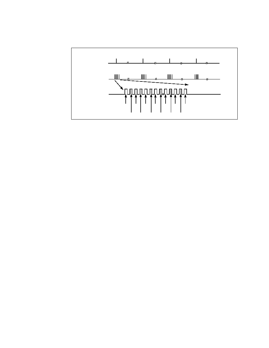
Figure 1.7
.
Figure 1.7 NLP vs FLP Link Pulse
Any of the following events initiates the AutoNegotiation algorithm:
∑
Power up
∑
Device reset
∑
The AutoNegotiation Enable (ANEG_EN) bit in the MI serial port Control register
for that port is cleared, then set
∑
The AutoNegotiation Reset (ANEG_RST) bit in the MI serial port Control register
is set
∑
The channel enters the Link Fail state
Once a negotiation has been initiated, the device first determines if the remote device
has AutoNegotiation capability. If the remote device is not AutoNegotiation capable
and is just transmitting either 10BASE-T or 100BASE-TX signals, the device senses
it and places itself in the same mode as the remote device.
If the device detects FLPs from the remote device, the remote device is determined
to have AutoNegotiation capability, and the device then uses the contents of the MI
serial port AutoNegotiation Advertisement register for that port to advertise its
capabilities to the remote device.
The remote device does the same, and the capabilities read back from the remote
device are stored in the MI serial port AutoNegotiation Remote End Capability
register. The LAN83C183 negotiation algorithm then matches its capabilities to the
remote device's capabilities and determines the device configuration according to the
priority resolution algorithm defined in IEEE 802.3 Clause 28.
When the negotiation process is completed, the LAN83C183 then configures itself
for either 10 or 100 Mbits/s mode and either Full- or Half-Duplex modes (depending
on the outcome of the negotiation process), and it switches to either the 100BASE-
TX or 10BASE-T link integrity algorithms (depending on which mode was enabled
through AutoNegotiation). Refer to IEEE 802.3 Clause 28 for more details.
1.2.11.4 AUTONEGOTIATION OUTCOME INDICATION
The outcome or result of the AutoNegotiation process is stored in the 10/100 Speed
Detect (SPD_DET) and Duplex Detect (DPLX_DET) bits in the MI serial port Status
Output register.
Normal Link Pulse (NLP)
TPO±
TPO±
Fast Link Pulse (FLP)
Clock Clock Clock Clock Clock Clock Clock
Data Data Data Data Data Data
D0
D1
D2
D3
D14
D15

SMSC DS ≠ LAN83C183
34
Rev. 12/14/2000
1.2.11.5 AUTONEGOTIATION STATUS
To monitor the status of the AutoNegotiation process, simply read the AutoNegotiation
Acknowledgement (ANEG_ACK) bit in the MI serial port Status register. The
ANEG_ACK bit is 1 when an AutoNegotiation has been initiated and successfully
completed.
1.2.11.6 AUTONEGOTIATION ENABLE
To enable the AutoNegotiation algorithm, set the AutoNegotiation Enable bit
(ANEG_EN) in the MI serial port Control register, or assert the ANEG pin. To disable
the AutoNegotiation algorithm, clear the ANEG_EN bit, or deassert the ANEG pin.
When the AutoNegotiation algorithm is enabled, the device halts all transmissions
including link pulses for 1200 to 1500 ms, enters the Link Fail State, and restarts the
negotiation process. When the AutoNegotiation algorithm is disabled, the selection of
100 Mbits/s or
10 Mbits/s mode is determined with the SPEED bit in the MI serial port Control
register, and the selection of Half- or Full-Duplex mode determined from the state of
the DPLX bit in the MI serial port Control register.
1.2.11.7 AUTONEGOTIATION RESET
Appropriately setting the AutoNegotiation Reset (ANEG_RST) bit in the MI serial port
Control register can initiate or reset the AutoNegotiation algorithm at any time.
1.2.12 Link Indication
Receive link detect activity can be monitored through the Link Detect bit (LINK) in
the MI serial port Status register and the Link Fail Detect bit (LNK_FAIL) in the Status
Output register. Link detect activity can also be programmed to appear on the
PLED3n or PLED0n pins. To do this, appropriately set the Programmable LED Output
Select bits in the MI serial port Configuration 2 register as shown in
Table 1.9
. When
either the PLED3n or PLED0n pins are programmed to be a link detect output, they
are asserted LOW whenever the device is in the Link Pass State.
The PLED3 output is an open-drain pin with pullup resistor and can drive an LED
from V
DD
. The PLED0 output has both pullup and pulldown driver transistors in
addition to a weak pullup resistor, so it can drive an LED from either V
DD
or GND.
Both the PLED3n and PLED0n outputs can also drive another digital input. Refer to
Section 1.2.14, "LED Drivers," page 1-36
for a description on how to program the
PLED[3:0]n pins and their default values.

SMSC DS ≠ LAN83C183
35
Rev. 12/14/2000
1.2.13 Collision
Collisions occur whenever transmit and receive operations occur simultaneously
while the device is in Half-Duplex mode.
1.2.13.1 100 MBITS/S
In 100 Mbits/s operation, a collision occurs and is sensed whenever there is
simultaneous transmission (packet transmission on TPO+/-) and reception (non-idle
symbols detected at the TPI+/- input). When a collision is detected, the COL output
is asserted, TP data continues to be transmitted on the twisted-pair outputs, TP data
continues to be received on the twisted-pair inputs, and internal CRS loopback is
disabled. After a collision is in process, CRS is asserted and stays asserted until the
receive and transmit packets that caused the collision are terminated.
The collision function is disabled if the device is in the Full-Duplex mode, is in the
Link Fail state, or if the device is in the diagnostic loopback mode.
1.2.13.2 10 MBITS/S
A collision in the 10 Mbits/s mode is identical to one the 100 Mbits/s mode except:
∑
The 10 Mbits/s squelch criteria determines reception
∑
The RXD[3:0] outputs are all forced LOW
∑
The collision signal (COL) is asserted when the SQE test is performed
∑
The collision signal (COL) is asserted when the jabber condition has been
detected.
1.2.13.3 COLLISION TEST
To test the Controller Interface collision signal (COL), set the COLTST bit in the MI
serial port Control register. When this bit is set, TX_EN is looped back onto COL and
the TP outputs are disabled.
1.2.13.4 COLLISION INDICATION
Collisions are indicated through the COL pin, which is asserted HIGH every time a
collision occurs. The device can also be programmed to indicate collisions on the
PLED2n output.
In the MI serial port Configuration 2 register, set the LED function select bits
(LED_DEF_[1:0]) so that collision activity is indicated at the PLED2n output. Set the
PLED2_[1:0] bits in the same register to 0b11 (normal). With these settings, a LED
connected to the PLED2n pin will reflect collision activity.
When the PLED2n pin is programmed to be a collision detect output, it is asserted
LOW for 100 ms every time a collision occurs. The PLED2n output is open drain with
a pullup resistor and can drive an LED from V
DD
or can drive another digital input.
See
Section 1.2.14, "LED Drivers," page 1-36
for more details on how to program the
LED output pins to indicate various conditions.

SMSC DS ≠ LAN83C183
36
Rev. 12/14/2000
1.2.14 LED Drivers
The PLED[5:2]n outputs are open-drain with a pullup resistor and can drive LEDs
tied to V
DD
. The PLED[1:0]n outputs have both pullup and pulldown driver transistors
with a pullup resistor, so the PLED[1:0]n outputs can drive LEDs tied to either V
DD
or GND.
The PLED[5:0]n outputs can be programmed through the MI serial port Configuration
2 register for the following functions:
∑
Normal Function
∑
On
∑
Off
∑
Blink
The PLED[5:0]n outputs are programmed with the LED output select bits
(PLED_[1:0]) and the LED Normal Function select bits (LED_DEF[1:0]) in the MI
serial port Configuration register.
1.2.14.1 LED OUTPUT SELECT BITS
There are four sets of output select bits in MI serial port Configuration register, one
set for each LED output pin:
∑
PLED3_[1:0] control the PLED3n output
∑
PLED2_[1:0] control the PLED2n output
∑
PLED1_[1:0] control the PLED1n output
∑
PLED0_[1:0] control the PLED0n output
The PLEDx_[1:0] bits program the outputs to operate in the following modes:
∑
Normal operation (see
Section 1.2.14.2, "LED Normal Function Select Bits"
)
∑
Blink
∑
Steady On (PLED[3:0]n pin LOW)
∑
Steady Off (PLED[3:0]n pin HIGH)
Table 1.8
shows the encoding of the output select bits.
1.2.14.2 LED NORMAL FUNCTION SELECT BITS
When the PLED[5:0]n pins are programmed for their normal functions (PLED_[1:0] =
0b11), the pin output states indicate four specific types of events. The LED Normal
Table 1.8 PLED_[1:0] Output Select Bit Encoding
PLED_[1]
PLED_[0]
LED State
LED Pin
1
1
Normal
LED pin reflects the functions selected with the
LED_DEF[1:0] bits
1
0
LED Blink
LED output driver continuously toggles at a rate of
100 ms on, 100 ms off
0
1
LED On
LED output driver is LOW
0
0
LED Off
LED output driver is HIGH

SMSC DS ≠ LAN83C183
37
Rev. 12/14/2000
Function select bits (LED_DEF[1:0]) in the MI serial port Configuration register
determine the states of the pins, as indicated in
Table 1.9
and
Table 1.10
.
The default Normal Functions for PLED[5:0]n are Receive Activity, Transmit Activity,
Link 100, Activity, Full Duplex, and Link 10, respectively.
Table 1.9 LED Normal Function Definition
LED_DEF[1:0]
PLED5n
PLED4n
PLED3n
PLED2n
PLED1n
PLED0n
0b11
RCV ACT
XMT ACT
LINK
COL
FDX
10/100
0b10
RCV ACT
XMT ACT
LINK
ACT
FDX
10/100
0b01
RCV ACT
XMT ACT
LINK + ACT
COL
FDX
10/100
0b00
1
RCV ACT
XMT ACT
LINK 100
ACT
FDX
LINK10
1. The LAN83C183 powers up with the LED_DEF[1:0] bits set to the default value of 0b00.
Table 1.10 LED Event Definition
Symbol Definition
RCV ACT
Receive activity occurred, stretch pulse to 100 ms
XMT ACT
Transmit activity occurred, stretch pulse to 100 ms
LINK
100 or 10 Mbits/s link detected
LINK+ACT
100 or 10 Mbits/s link detected or activity occurred, stretch
pulse to 100 ms (link detect causes LED to be on, activity
causes LED to blink)
ACT
Activity occurred, stretch pulse to 100 ms
LINK100
100 Mbit/s link detected
COL
Collision occurred, stretch pulse to 100 ms
FDX
Full-Duplex mode enabled
10/100
10 Mbits/s mode enabled (HIGH), or 100 Mbits/s mode
enabled (LOW)
LINK10
10 Mbits/s link detected

SMSC DS ≠ LAN83C183
38
Rev. 12/14/2000
1.3 START OF PACKET
This section describes start of packet operation for both the 100 Mbits/s and 10
Mbits/s modes.
1.3.1 100 Mbits/s
A unique Start of Stream Delimiter (SSD) indicates the start of packet for 100 Mbits/s
mode. The SSD pattern consists of two /J/K/ 5B symbols inserted at the beginning
of the packet in place of the first two preamble symbols, as defined in IEEE 802.3
Clause 24 and shown in
Table 1.4
and
Figure 1.2
.
The 4B5B encoder generates the transmit SSD and inserts the /J/K/ symbols at the
beginning of the transmit data packet in place of the first two 5B symbols of the
preamble, as shown in
Figure 1.2
.
The 4B5B decoder detects the receive pattern. To do this, the decoder examines
groups of 10 consecutive code bits (two 5B words) from the descrambler. Between
packets, the receiver detects the idle pattern
(5B /I/ symbols). When in the idle state, the device deasserts the CRS and RX_DV
pins.
If the receiver is in the idle state and 10 consecutive code bits from the receiver
consist of the /J/K/ symbols, the start of packet is detected, data reception begins,
and /5/5/ symbols are substituted in place of the /J/K/ symbols.
If the receiver is in the idle state and 10 consecutive code bits from the receiver are
a pattern that is neither /I/I/ nor /J/K/ symbols, but contain at least two noncontiguous
zeros, activity is detected but the start of packet is considered to be faulty and a
False Carrier Indication (also referred to as bad SSD) is signaled to the controller
interface.
When False Carrier is detected, CRS is asserted, RX_ER is asserted, RX_DV
remains deasserted, the RXD[3:0] output state is 0b1110 while RX_ER is asserted,
and the Start of Stream Error bit (SSD) is set in the MI serial port Status Output
register. Once a False Carrier Event is detected, the idle pattern (two /I/I/ symbols)
must be detected before any new SSDs can be sensed.
If the receiver is in the idle state and 10 consecutive code bits from the receiver
consist of a pattern that is neither /I/I/ nor /J/K/ symbols but does not contain at least
two noncontiguous zeros, the data is ignored and the receiver stays in the idle state.
1.3.2 10 Mbits/s
Because the idle period in 10 Mbits/s mode is defined to be when there is no valid
data on the TP inputs, the start of packet for 10 Mbits/s mode is detected when the
TP squelch circuit detects valid data. When the start of packet is detected, CRS is
asserted as described in
Section 1.2.2, "Controller Interface," page 1-16
. See
Section
1.2.8.4, "Squelch (10 Mbits/s)," page 1-29
for details on the squelch algorithm.

SMSC DS ≠ LAN83C183
39
Rev. 12/14/2000
1.4 END OF PACKET
This section describes end of packet operation for both the 100 Mbits/s and 10
Mbits/s modes.
1.4.1 100 Mbits/s
The End of Stream Delimiter (ESD) indicates the end of packet for 100 Mbits/s mode.
The ESD pattern consists of two /T/R/ 4B5B symbols inserted after the end of the
packet, as defined in IEEE 802.3 Clause 24 and shown in
Table 1.4
and
Figure 1.2
.
The 4B5B encoder generates the transmit ESD and inserts the /T/R/ symbols after
the end of the transmit data packet, as shown in
Figure 1.2
.
The 4B5B decoder detects the ESD pattern when there are groups of 10 consecutive
code bits (two 5B words) from the descrambler during valid packet reception.
If the 10 consecutive code bits from the receiver during valid packet reception consist
of the /T/R/ symbols, the end of packet is detected, data reception is terminated, the
CRS and RX_DV pins are asserted, and /I/I/ symbols are substituted in place of the
/T/R/ symbols.
If 10 consecutive code bits from the receiver during valid packet reception do not
consist of /T/R/ symbols, but instead consist of /I/I/ symbols, the packet is considered
to have been terminated prematurely and abnormally, and the end of packet
condition is signalled to the controller interface.
When the premature end of packet condition is detected, the RX_ER signal is
asserted for the nibble associated with the first /I/ symbol detected, then the CRS
and RX_DV pins are deasserted.
The device also sets End of Stream Error bit (ESD) in the MI serial port Status Output
register to indicate the premature end of packet condition.
1.4.2 10 Mbits/s
The end of packet for 10 Mbits/s mode is indicated with the SOI (Start of Idle) pulse.
The SOI pulse is a positive double wide pulse containing a Manchester code violation
inserted at the end of every packet.
The TP transmitter generates the transmit SOI pulse and inserts it at the end of the
data packet after TX_EN has been deasserted. The transmit waveshaper shapes the
transmitted SOI output pulse at the TP output to meet the pulse template
requirements specified in IEEE 802.3 Clause 14 and shown in
Figure 1.8
.
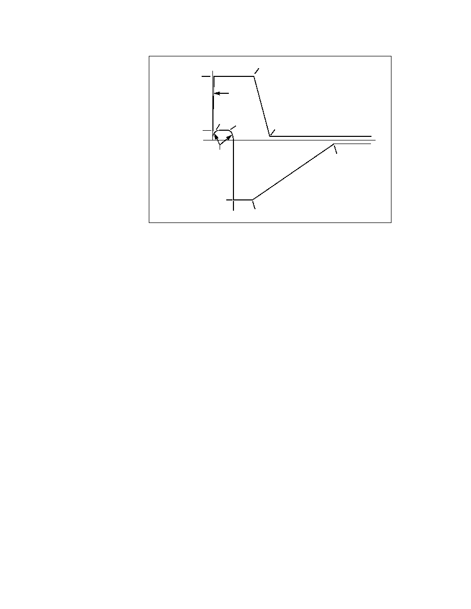
SMSC DS ≠ LAN83C183
40
Rev. 12/14/2000
Figure 1.8 SOI Output Voltage Template - 10 Mbits/s
The TP receiver senses missing data transitions in order to detect the receive SOI
pulse. Once the SOI pulse is detected, data reception is ended and the CRS and
RX_DV pins are deasserted.
0 BT
4.5 BT
6.0 BT
+ 50 mV
-
50 mV
45.0 BT
4.5 BT
2.5 BT
-
3.1 V
0.25 BT
2.25 BT
585 mV
3.1 V
0.5 V/ns
585 mV sin (2
(t/1 BT))
0
t
0.25 BT and
225
t
2.5 BT

SMSC DS ≠ LAN83C183
41
Rev. 12/14/2000
1.5 FULL/HALF DUPLEX MODE
Half-Duplex mode is the CSMA/CD operation defined in IEEE 802.3. It allows
transmission or reception, but not both at the same time. Full-Duplex operation is a
mode that allows simultaneous transmission and reception. Full duplex in the 10
Mbits/s mode is identical to operation in the 100 Mbits/s mode.
The device can be forced into either the Full- or Half-Duplex mode, or the device can
use AutoNegotiation to autoselect Full/Half-Duplex operation. When the device is
placed in Full-Duplex mode:
∑
The collision function is disabled, and
∑
TX_EN to CRS loopback is disabled
1.5.1 Forcing Full/Half Duplex Operation
To independently force a channel into either the Full- or Half-Duplex mode, set the
Duplex Mode Select (DPLX) bit in the MI serial port Control register, or assert the
DPLX pin, assuming that AutoNegotiation is not enabled with the ANEG_EN bit in
the MI serial port Control register.
The device automatically configures itself for Full- or Half-Duplex mode. To do this,
the device uses the AutoNegotiation algorithm to advertise and detect Full and Half
Duplex capabilities to and from a remote device. To enable AutoNegotiation, set the
AutoNegotiation Enable (ANEG_EN) bit in the MI serial port Control register or assert
the ANEG pin.
To select the advertised Full/Half Duplex capability, appropriately set the bits in the
MI serial port AutoNegotiation Advertisement register. AutoNegotiation functionality is
described in more detail in
Section 1.2.11, "Link Integrity and AutoNegotiation"
.
1.5.2 Full/Half Duplex Indication
Full Duplex detection can be monitored through the Duplex Detect bit (DPLX_DET)
in the MI serial port Status Output register.
The device can also be programmed such that the Full-Duplex indication appears on
the PLED1n pin. To do this, appropriately set the Programmable LED Output Select
bits in the MI serial port Configuration 2 register as described in
Table 1.9
. When the
PLED1n pin is programmed to be a Full-Duplex detect output, it is asserted LOW
when the device is configured for Full Duplex operation. The PLED1 output has both
pullup and pulldown driver transistors and a weak pullup resistor, so it can drive an
LED from either V
DD
or GND and can also drive a digital input.
1.5.3 Loopback
1.5.3.1 INTERNAL CRS LOOPBACK
TX_EN is internally looped back onto CRS during every transmit packet. This internal
CRS loopback is disabled during collision, in Full-Duplex mode, in the Link Fail State,
and when the Transmit Disable bit (XMT_DIS) is set in the MI serial port
Configuration 1 register. In 10 Mbits/s mode, internal CRS loopback is also disabled
when jabber is detected.
1.5.3.2 DIAGNOSTIC LOOPBACK
Setting the loopback bit (LPBK) in the MI serial port Control register selects the
diagnostic loopback mode. When diagnostic loopback is enabled, the TXD[3:0] data
is looped back onto RXD[3:0], TX_EN is looped back onto CRS, RX_DV operates
normally, the TP receive and transmit paths are disabled, the transmit link pulses are

SMSC DS ≠ LAN83C183
42
Rev. 12/14/2000
halted, and the Half/Full Duplex modes do not change. Diagnostic loopback cannot
be enabled when in the FBI mode (see
Section 1.2.2.2, "FBI Interface," page 1-19
).
1.6 REPEATER MODE
The LAN83C183 uses the standard MII as the physical interface for MII-based
repeater cores.
The LAN83C183 has one predefined repeater mode. To enable this mode, assert the
RPTR pin. When this repeater mode is enabled with the RPTR pin:
∑
TX_EN to CRS loopback is disabled
∑
AutoNegotiation is disabled
∑
100 Mbits/s operation is enabled
∑
Half-Duplex operation is enabled
Note:
Enabling the repeater mode with the RPTR pin is only one of many pos-
sible repeater modes available on the device. Other repeater modes
are available when appropriate register bits are set to enable or disable
the desired functions for a given repeater mode type.
For additional information, see ?Application Note?.
1.7 10/100 MBITS/S SELECTION
The device can be forced into either the 10 or 100 Mbits/s mode, or it can use
AutoNegotiation to autoselect 10 or 100 Mbits/s operation.
1.7.1 Forcing 10/100 Mbits/s Operation
To independently force each channel into either the 10 Mbits/s or 100 Mbits/s mode:
∑
Clear the ANEG_EN bit in the MI serial port Control register, and
∑
Appropriately set the Speed Select (SPEED) bit in the MI serial port Control
register.
Alternatively, if the ANEG pin is LOW, the SPEED pin controls the speed. Asserting
the SPEED pin HIGH forces 100 Mbits/s operation and deasserting it LOW forces 10
Mbits/s operation.
1.7.2 Autoselecting 10/100 Mbits/s Operation
The device can automatically configure itself for 10 or 100 Mbits/s mode. To do this,
it uses the AutoNegotiation algorithm to advertise and detect 10 and 100 Mbits/s
capabilities to and from a remote device. Setting the AutoNegotiation Enable
(ANEG_EN) bit in the MI serial port Control register enables AutoNegotiation.
Appropriately setting the bits in the MI serial port AutoNegotiation Advertisement
register selects the advertised speed capability. AutoNegotiation functionality is
described in more detail in
Section 1.2.11, "Link Integrity and AutoNegotiation"
.
1.7.3 10/100 Mbits/s Indication
The device can be programmed such that the operation speed (10 or 100 Mbits/s)
appears on the PLED0n pin. To do this, appropriately set the Programmable LED Out-
put Select bits in the MI serial port Configuration 2 register as described in
Table 1.9
.
When the PLED0n pin is programmed to be speed detect output, it is asserted LOW
when the device is configured for 100 Mbit/s operation. The PLED0n output has both
pullup and pulldown driver transistors and a weak pullup resistor, so it can drive an
LED from either V
DD
or GND and can also drive a digital input.

SMSC DS ≠ LAN83C183
43
Rev. 12/14/2000
1.8 JABBER
A jabber condition occurs in 10 Mbits/s mode when the transmit packet exceeds a
predetermined length. When jabber is detected, the TP transmit outputs are forced
to the idle state, a collision is asserted, the JAB register bit is set in the MI serial port
Status register, and the JAB bit is set in the MI serial port Status Output register.
To disable the jabber function, set the Jabber Disable bit (JAB_DIS) in the MI serial
port Configuration 2 register
The jabber function is disabled in the 100 Mbits/s mode.
1.9 AUTOMATIC JAM
This section describes automatic JAM operation for both 100 and 10 Mbits/s
operation.
1.9.1 100 Mbits/s JAM
The LAN83C183 has an automatic JAM feature that causes the device to
automatically transmit a JAM packet if receive activity is detected. If automatic JAM
is enabled, the following JAM packet is transmitted on TPO± when the RX_EN/JAMn
pin is asserted LOW and receive activity is detected on the TP inputs (expressed in
5B code words):
/J/K/5/5/5/5/5/5/5/5/5/5/5/5/5/D/H/H/H/H/H/H/H/H/T/R/
This automatic JAM feature is enabled when the RX_EN/JAM pin is programmed to
be a JAM input. To configure the RX_EN/JAMn pin as a JAMn input, set the
R/J_CFG bit in the MI serial port Configuration 2 register.
1.9.2 10 Mbits/s JAM
The JAM feature for the 10 Mbits/s mode is identical to that of the 100 Mbits/s mode
except that the JAM packet transmitted on TPO± consists of the standard 62-bit
preamble (alternating 1s and 0s) followed with the SFD pattern (0b11), which is then
followed with 32 bits of alternating 1s and 0s.

SMSC DS ≠ LAN83C183
44
Rev. 12/14/2000
1.10 RESET
The device is reset when:
1.
V
DD
is applied to the device, or
2.
The reset bit (RST) is set in the MI serial port Control register, or
3.
The RESETn pin is asserted (LOW).
When reset occurs because of (1) or (2), an internal power-on reset pulse is
generated that resets all internal circuits, forces the MI serial port bits to their default
values, and latches in new values for the MI address. After the power-on reset pulse
has finished, the reset bit (RST) in the MI serial port Control register is cleared and
the device is ready for normal operation.
When reset is initiated because of (3), the same procedure occurs except the device
stays in the reset state as long as the RESETn pin is held LOW. The RESETn pin
has an internal pullup to V
DD
. The device is guaranteed to be ready for normal
operation 50 ms after the reset sequence is initiated.
1.11 POWERDOWN
To powerdown the LAN83C183, set the Powerdown bit (PDN) in the MI serial port
Control register. In powerdown mode, the TP outputs are in a
high-impedance state, all functions are disabled except the MI serial port, and the
power consumption is reduced to a minimum. The device is guaranteed to be ready
for normal operation 500 ms after the PDN bit is cleared.
1.12 RECEIVE POLARITY CORRECTION
In 10 Mbits/s mode, the polarity of the signal on the TP receive input is continuously
monitored. If either three consecutive link pulses or one SOI pulse indicates incorrect
polarity on the TP receive input, the polarity is internally determined to be incorrect.
In this case, the Reverse Polarity Detect bit (RPOL) is set in the MI serial port Status
Output register.
The device automatically corrects for the reverse polarity condition, provided the
autopolarity feature is not disabled. To disable autopolarity, set the Autopolarity
Disable bit (APOL_DIS) in the MI serial port Configuration 2 register.
No polarity detection or correction is needed in the 100 Mbits/s mode.
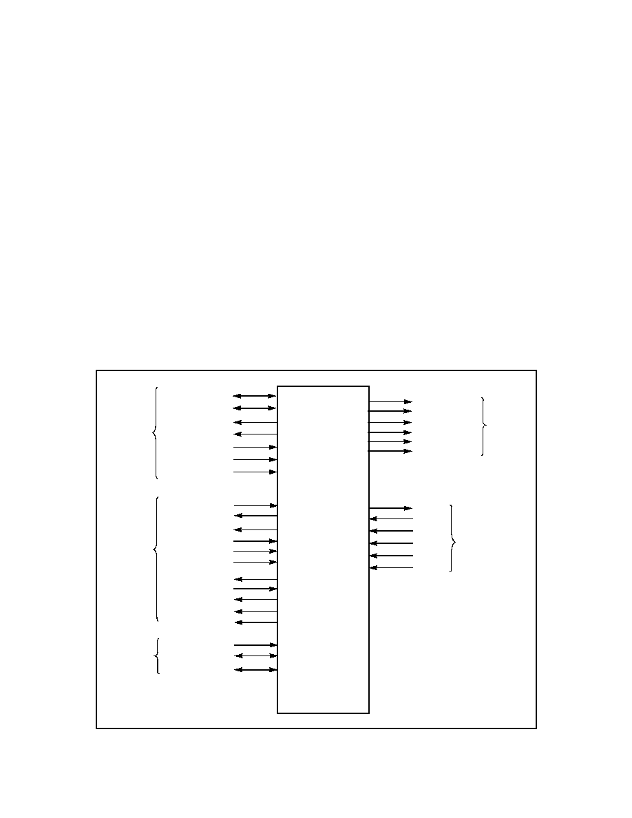
SMSC DS ≠ LAN83C183
45
Rev. 12/14/2000
Chapter 2
Signal Descriptions
This chapter describes the device signals. It contains the following sections:
∑
Section 2.1, "Media Interface Signals"
∑
Section 2.2, "Controller Interface Signals (MII)"
∑
Section 2.3, "Management Interface"
∑
Section 2.4, "Miscellaneous Signals"
∑
Section 2.5, "LEDs"
∑
Section 2.6, "Power Supply"
Figure 2.1
is a logic diagram for the device.
Figure 2.1 Device Logic Diagram
Media
Interface
OSCIN
TX_EN
Controller
Interface
Management
Interface
MDC
MDIO
PLED3n/MDA3n
PLED2n/MDA2n
PLED1n/MDA1n
LEDs/
COL
RESETn
Miscellaneous
10/100 Mbit/s
Ethernet
Physical Layer
Device (PHY)
(MII)
TPI+/FXO-
TPI-/FXO+
TPO+/FXI-
TPO-/FXI+
TX_ER/TXD4
TXD[3:0]
RXD[3:0]
RX_EN/JAMn
RX_CLK
TX_CLK
RX_DV
PLED0n/MDA0n
RX_ER/RXD4
MI Address
CRS
SPEED
REXT
DPLX
ANEG
RPTR
SD/FXDISn
SD_THR
MDINTn/MDA4n
PLED4n
PLED5n
LAN83C183

SMSC DS ≠ LAN83C183
46
Rev. 12/14/2000
2.1 MEDIA INTERFACE SIGNALS
REXT
Transmit Current Set
I/O
An external resistor connected between the REXT pin and GND sets
the output current for the TP and FX
transmit outputs.
SD/FXDISn
I
FX Signal Detect Input/FX Interface Disable
When this pin is not tied to GND, the FX interface is enabled and this
pin becomes an ECL signal detect input. The voltage on SD_THR
determines the trip point for this ECL input.
When this pin is tied to GND, the FX interface is disabled and the TP
interface is enabled.
SD_THR
Signal Detect Input Threshold Level Set
I
The voltage on this pin determines the ECL threshold level (trip point)
for the SD input pin so that the device can directly interface to both
3.3 V and 5 V fiber optic transceivers. Typically, this pin is either tied
to GND (for 3.3 V operation) or to an external voltage divider (for 5
V operation).
TPO+/FXI-
Twisted-Pair Transmit Output (Positive), or
Fiber Optic Receive Input (Negative)
I/O
The TPO+/FXI- pin is shared for the twisted-pair and fiber optic sig-
nals. It functions as the positive signal in the twisted-pair output or
the negative signal in the fiber optic input.
TPO-/FXI+
Twisted-Pair Transmit Output (Negative), or
Fiber Optic Receive Input (Positive)
I/O
The TPO-/FXI+ pin is shared for the twisted-pair and fiber optic sig-
nals. It functions as the negative signal in the twisted-pair output or
the positive signal in the fiber optic input.
TPI+/FXO-
Twisted-Pair Receive Input (Positive), or
Fiber Optic Transmit Output (Negative)
I/O
The TPI+/FXO- pin is shared for the twisted-pair and fiber optic sig-
nals. It functions as the positive signal in the twisted-pair input or the
negative signal in the fiber optic output.
TPI-/FXO+
Twisted-Pair Receive Input (Negative), or
Fiber Optic Output (Positive)
I/O
The TPI-/FXO+ pin is shared for the twisted-pair and fiber optic sig-
nals. It functions as the negative signal in the twisted-pair input or the
positive signal in the fiber optic output.

SMSC DS ≠ LAN83C183
47
Rev. 12/14/2000
2.2 CONTROLLER INTERFACE SIGNALS (MII)
CRS
Carrier Sense Output
O
The CRS output is asserted HIGH when valid data is detected on the
receive TP inputs. CRS is clocked out on the falling edge of RX_CLK.
OSCIN
Clock Oscillator Input
I
There must be either a 25 MHz crystal between this pin and GND or
a 25 MHz clock applied to this pin. TX_CLK output is generated from
this input.
RX_CLK
Receive Clock Output
O
Receive data on RXD, RX_DV, and RX_ER is clocked out to an
external controller on the falling edge of RX_CLK.
RXD[3:0]
Receive Data Output
O
RXD[3:0] contain receive nibble data from the TP input, and they are
clocked out on the falling edge of RX_CLK.
RX_DV
Receive Data Valid Output
O
RX_DV is asserted HIGH when valid decoded data is present on the
RXD outputs. RX_DV is clocked out on the falling edge of RX_CLK.
RX_EN/JAMn Receive Enable Input
I
The function of this pin is configured through the R/J Configuration
Select bit (R/J_CFG) in the MI serial port Configuration 1 register.
When R/J_CFG is set, the pin is configured as JAMn; when it is
cleared, the pin functions as RX_EN
RX_EN function: when RX_EN is HIGH, all of the receive outputs
(RX_CLK, RXD[3:0], RX_DV, RX_ER, COL) are enabled. When
RX_EN is LOW, the outputs are in a
high-impedance state.
JAMn function: when JAMn is HIGH, a JAM packet is transmitted
when receive activity is detected. When JAMn is LOW, no JAM
packet is transmitted.
RXER/RXD4
Receive Error Output/Fifth Receive Data Output
O
The RXER/RXD4 output is asserted HIGH when a coding error or
other specified errors are detected on the receive twisted-pair inputs.
The signal is clocked out on the falling edge of RX_CLK.
If the device is placed in the Bypass 4B5B Decoder mode (the
BYP_ENC bit is set in the MI serial port Configuration 1 register), this
pin is reconfigured to be the fifth RXD receive data output, RXD4.
TX_CLK
Transmit Clock Output
O
Transmit data from the controller on TXD, TX_EN, and TX_ER is
clocked in on the rising edge of TX_CLK and OSCIN.
TXD[3:0]
Transmit Data Input
I
TXD[3:0] contain input nibble data to be transmitted on the TP out-
puts, and they are clocked in on the rising edge of TX_CLK and
OSCIN when TX_EN is asserted.

SMSC DS ≠ LAN83C183
48
Rev. 12/14/2000
TX_EN
Transmit Enable Input
I
TX_EN must be asserted HIGH to indicate that data on TXD and
TX_ER is valid. TX_ER is clocked in on the rising edge of TX_CLK
and OSCIN.
TX_ER/TXD4 Transmit Error Input/Fifth Transmit Data Input
I
The TXER pin, when asserted, causes a special pattern to be trans-
mitted on the twisted-pair outputs in place of normal data, and it is
clocked in on the rising edge of TX_CLK when TX_EN is asserted.
If the device is placed in the Bypass 4B5B Encoder mode (the
BYP_ENC bit is set in the MI serial port Configuration 1 register), this
pin is reconfigured to be the fifth TXD transmit data input, TXD4.
2.3 MANAGEMENT INTERFACE
MDC
MI Clock
I
The MDC clock shifts serial data for the internal registers into and out
of the MDIO pin on its rising edge.
MDINTn/MDA4n
Management Interface Interrupt Output/
Management Interface Address Input Pullup O.D. I/O
This pin is an interrupt output and is asserted LOW whenever there
is a change in certain MI serial port register bits. The pin is deas-
serted after all changed bits have been read out.
During powerup or reset, this pin is high impedance and the state of
the pin is latched in as the physical device address MDA4 for the MI
serial port.
MDIO
MI Data
I/O
This bidirectional pin contains serial data for the internal registers.
The data on this pin is clocked in and out of the device on the rising
edge of MDC.
2.4 MISCELLANEOUS SIGNALS
ANEG
AutoNegotiation Input
I
This pin control AutoNegotiation operation.
ANEG Pin
Meaning
HIGH
AutoNegotiation is on.
AutoNegotiation Enable is controlled
from the ANEG_EN bit, 10/100 Mbits/s
operation is controlled from the
SPEED bit, and Half/Full Duplex
operation is controlled from the DPLX
bit.
LOW
AutoNegotiation is off.
10/100 Mbits/s operation is controlled
from the SPEED pin and Half/Full
Duplex operation is controlled from the
DPLX pin.

SMSC DS ≠ LAN83C183
49
Rev. 12/14/2000
COL
Collision Output
O
COL is asserted HIGH when a collision between transmit and receive
data is detected.
DPLX
Full/Half Duplex Select Input
I
When the ANEG pin is LOW, the DPLX pin selects Half/Full Duplex
operation.
When the ANEG pin is HIGH, the DPLX pin is ignored and the
Half/Full Duplex operation is controlled from the Duplex Mode Select
bit (DPLX) in the MI serial port Control register or the AutoNegotiation
outcome.
NC
No Connect
--
13 of the pins are not connected.
RESETn
Hardware Reset Input
Pullup I
RPTR
Repeater Mode Enable Input
I
The RPTR pin controls the device repeater operation.
SPEED
Speed Select Input
I
When the ANEG pin is LOW, the SPEED pin selects 10/100 Mbits/s
operation.
When the ANEG pin is HIGH, this pin is ignored and the speed is
determined from the Speed Select bit (SPEED) in the MI serial port
Control register or the
AutoNegotiation outcome.
DUPLX Pin
Meaning
HIGH
Full Duplex operation
LOW
Half Duplex operation
RESETn Pin
Meaning
HIGH
Normal
LOW
Device is in a reset state.
RPTR Pin
Meaning
HIGH
Repeater mode enabled
LOW
Normal operation
SPEED Pin
Meaning
HIGH
100 Mbits/s operation
LOW
10 Mbits/s operation

SMSC DS ≠ LAN83C183
50
Rev. 12/14/2000
2.5 LEDS
PLED5n
Receive LED Output Pullup O.D.
O
The function of this pin is to be a Receive Activity Detect output. The
pin can drive an LED from V
DD
.
PLED4n
Transmit LED Output Pullup O.D.
O
The function of this pin is to be a Transmit Activity Detect output. The
pin can drive an LED from V
DD
.
PLED3n/MDA3n
Programmable LED Output/MI Address Bit
Pullup O.D. I/O
The default function of this pin is to be a 100 Mbits/s Link Detect out-
put. This pin can also be programmed through the MI serial port to
indicate other events or be user controlled. This pin can drive an LED
from V
DD
.
When programmed as a 100 Mbits/s Link Detect Output (default):
During powerup or reset, this pin is high-impedance and the level on
this pin is latched in as the physical device address MDA3n for the
MI serial port.
PLED2n/MDA2n
Programmable LED Output/MI Address Bit
Pullup O.D. I/O
The default function of this pin is to be an Activity Detect output. This
pin can also be programmed through the MI serial port to indicate
other events or be user controlled. This pin can drive an LED from
V
DD
.
When programmed as an Activity Detect Output (default):
During powerup or reset, this pin is high-impedance and the level on
this pin is latched in as the physical device address MDA2n for the
MI serial port.
PLED5n
Pin
Function
HIGH
No receive activity
LOW
Receive packet occurred (held LOW for 100 ms)
PLED4n
Pin
Function
HIGH
No transmit activity
LOW
Transmit packet occurred (held LOW for 100 ms)
PLED3n/MDA3n
Pin
Function
HIGH
No Link Detect
LOW
100 Mbits/s Link Detected
PLED2n/MDA2n
Pin
Function
HIGH
No Activity
LOW
Transmit or receive packet
occurred (held LOW for 100 ms)

SMSC DS ≠ LAN83C183
51
Rev. 12/14/2000
PLED1n/MDA1n
Programmable LED Output/MI Address Bit
Pullup O.D. I/O
The default function of this pin is to be a Full Duplex Detect output.
This pin can also be programmed through the MI serial port to indi-
cate other events or be user controlled. This pin can drive an LED
from both V
DD
and GND.
When programmed as Full Duplex Detect Output (default):
During powerup or reset, this pin is high-impedance and the level on
this pin is latched in as the physical address device address MDA1n
for the MI serial port.
PLED0n/MDA0n
Programmable LED Output/MI Address Bit
Pullup O.D. I/O
The default function of this pin is to be a 10 Mbits/s Link Detect out-
put. This pin can also be programmed through the MI serial port to
indicate other events or be user controlled. This pin can drive an LED
from both V
DD
and GND.
When programmed as 10 Mbits/s Link Detect Output (default):
During powerup or reset, this pin is high-impedance and the value on
this pin is latched in as the address MDA0n for the MI serial port.
2.6 POWER SUPPLY
GND
Ground
I
There are six ground pins. They must be connected to ground (0
Volts).
V
DD
Positive Supply
I
There are six V
DD
pins. They must be connected to
3.3
±
5% Volts.
PLED1n/MDA1n
Pin
Function
HIGH
Half-Duplex
LOW
Full-Duplex
PLED0n/MDA0n
Pin
Function
HIGH
No Detect
LOW
10 Mbits/s Link Detected

SMSC DS ≠ LAN83C183
52
Rev. 12/14/2000

SMSC DS ≠ LAN83C183
53
Rev. 12/14/2000
Chapter 3
Registers
This chapter contains a description of the registers accessed over the management
interface (MI) serial interface. It contains the following sections:
∑
Section 3.1, "Bit Types"
∑
Section 3.2, "MI Serial Port Register Summary"
∑
Section 3.3, "Registers"
For further information about the operation of the MI serial interface, see
Chapter 4,
Management Interface
.

SMSC DS ≠ LAN83C183
54
Rev. 12/14/2000
3.1 BIT TYPES
Because the serial port is bidirectional (capable of both read and write operations),
there are many types of bits. The following bit type definitions are summarized in
Table 3.1
:
∑
Write bits (W) are inputs during a write cycle and are high impedance during a
read cycle
∑
Read bits (R) are outputs during a read cycle and high impedance during a write
cycle
∑
Read/Write bits (R/W) are actually write bits that can be read out during a read
cycle
∑
R/WSC bits are R/W bits that are self-clearing after a set period of time or after
a specific event has completed
∑
R/LL bits are read bits that latch themselves when they go LOW, and they stay
LOW until read. After they are read, they are reset HIGH.
∑
R/LH bits are the same as R/LL bits, except that they latch HIGH.
∑
R/LT are read bits that latch themselves whenever they make a transition or
change value, and they stay latched until they are read. After R/LT bits are read,
they are updated to their current value.
Table 3.1 MI Register Bit Type Definition
Symbol
Name
Definition
Write Cycle
Read Cycle
W
Write
Input
No operation, Hi-Z
R
Read
No operation, Hi-Z
Output
R/W
Read/Write
Input
Output
R/WSC
Read/Write, Self-Clearing
Input
Output
(clears itself
after the operation completes)
R/LL
Read/Latching LOW
No operation, Hi-Z
Output
When the bit goes LOW, it is latched.
When the bit is read, it is updated.
R/LH
Read/Latching HIGH
No operation, Hi-Z
Output
When the bit goes HIGH, it is latched.
When the bit Is read, it is updated.
R/LT
Read/Latching on transition
No operation, Hi-Z
Output
When the bit transitions, the bit is latched.
When the bit is read, the bit is updated.

SMSC DS ≠ LAN83C183
55
Rev. 12/14/2000
3.2 MI SERIAL PORT REGISTER SUMMARY
The following tables summarize the device registers accessible through the MI serial
port.
Control Register (register 0) ≠
Status Register (register 1) ≠
PHY ID #1 Register (register 2) ≠
PHY ID #2 Register (register 3) ≠
AutoNegotiation Advertisement Register (register 4) ≠
AutoNegotiation Remote End Capability Register (register 5) ≠
15
14
13
12
11
10
9
8
RST
LPBK
SPEED
ANEG_EN
PDN
MII_DIS
ANEG_RST
DPLX
7
6
0
COLTST
Reserved
15
14
13
12
11
10
8
CAP_T4
CAP_TXF
CAP_TXH
CAP_TF
CAP_TH
Reserved
7
6
5
4
3
2
1
0
Reserved
CAP_SUPR ANEG_ACK
REM_FLT
CAP_ANEG
LINK
JAB
EXREG
15
14
13
12
11
10
9
8
OUI3
OUI4
OUI5
OUI6
OUI7
OUI8
OUI9
OUI10
7
6
5
4
3
2
1
0
OUI11
OUI12
OUI13
OUI14
OUI15
OUI16
OUI17
OUI18
15
14
13
12
11
10
9
8
OUI19
OUI20
OUI21
OUI22
OUI23
OUI24
PART5
PART4
7
6
5
4
3
2
1
0
PART3
PART2
PART1
PART0
REV3
REV2
REV1
REV0
15
14
13
12
10
9
8
NP
ACK
RF
Reserved
T4
TX_FDX
7
6
5
4
1
0
TX_HDX
10_FDX
10_HDX
Reserved
CSMA
15
14
13
12
10
9
8
NP
ACK
RF
Reserved
T4
TX_FDX
7
6
5
4
1
0
TX_HDX
10_FDX
10_HDX
Reserved
CSMA

SMSC DS ≠ LAN83C183
56
Rev. 12/14/2000
Configuration 1 Register (register 16) ≠
Configuration 2 Register (register 17) ≠
Status Output Register (register 18) ≠
Mask Register (register 19)
Reserved Register (register 20) ≠
15
14
13
12
11
10
9
8
LINK_DIS
XMT_DIS
XMT_PDN TXEN_CRS BYP_ENC
BYP_SCR
UNSCR_DIS
EQLZR
7
6
5
2
1
0
CABLE
RLVL0
TLVL[3:0]
TRF[1:0]
15
14
13
12
11
10
9
8
PLED3_1
PLED3_0
PLED2_1
PLED2_0
PLED1_1
PLED1_0
PLED0_1
PLED0_0
7
6
5
4
3
2
1
0
LED_DEF1 LED_DEF0
APOL_DIS
JAB_DIS
MREG
INT_MDIO
R/J_CFG
0
15
14
13
12
11
10
9
8
INT
LINK_FAIL LOSS_SYNC
CWRD
SSD
ESD
RPOL
JAB
7
6
5
0
SPD_DET
DPLX_DET
Reserved
15
14
13
12
11
10
9
8
MASK_INT
MASK_LNK_FAIL
MASK_LOSS_SYNC MASK_CWRD MASK_SSD MASK_ESD MASK_RPOL MASK_JAB
7
6
5
4
3
0
MASK_SPD_DET MASK_DPLX_DET
FXLVL[1:0]
Reserved
15
14
13
12
11
10
9
8
Reserved
7
6
5
0
Reserved

SMSC DS ≠ LAN83C183
57
Rev. 12/14/2000
3.3 REGISTERS
This section contains a description of each of the bits in each register.
3.3.1 Control Register (Register 0)
The default value for this register is 0x3000.
RST
Reset
R/WSC 15
LPBK
Loopback Enable
R/W 14
SPEED
Speed Select
R/W 13
ANEG_EN AutoNegotiation Enable
R/W 12
PDN
Power Down Enable
R/W 11
MII_DIS
MII Interface Disable
R/W 10
15
14
13
12
11
10
9
8
RST
LPBK
SPEED
ANEG_EN
PDN
MII_DIS
ANEG_RST
DPLX
7
6
0
COLTST
Reserved
RST Bit
Meaning
1
Reset. The bit is bit self-clearing in less than or
equal to 200
µ
s after reset finishes.
0
Normal (Default)
LPBK Bit
Meaning
1
Loopback mode enabled
0
Normal (Default)
SPEED Bit
1
1. The SPEED bit is effective only when AutoNegotiation is off,
and the bit can be overridden with the assertion of the
SPEED pin.
Meaning
1
100 Mbit/s (100BASE-TX) (default)
0
10 Mbit/s (10BASE-T)
ANEG_EN
Bit
1
1. The ANEG_EN pin can be overridden with the
assertion of the ANEG pin.
Meaning
1
1 = AutoNegotiation enabled (default)
0
0 = Disabled
PDN Bit
Meaning
1
Power down
0
Normal (default)
MII_DIS
1
Bit
1. If MDA[3:0]n is not read as 0b1111 at reset
time, the MII_DIS default value is changed
to 0.
0
MII interface disable
1
Normal (default)

SMSC DS ≠ LAN83C183
58
Rev. 12/14/2000
ANEG_RSTAutoNegotiation Reset
R/WSC 9
DPLX
Duplex Mode Select
R/W 8
COLTST
Collision Test Enable
R/W 7
R
Reserved
R [6:0]
These bits are reserved and must be remain at the default value of
0x00 for proper device operation.
3.3.2 Status Register (Register 1)
The default value of this register is 0x7809.
CAP_T4
100BASE-T4 Capable
R 15
CAP_TXF 100BASE-TX Full Duplex Capable
R 14
CAP_TXH 100BASE-TX Half Duplex Capable
R 13
ANEG_RST Bit
1
Restart AutoNegotiation process. The bit is
self-clearing after reset is finished
0
Normal (default)
DPLX Bit
1
1. This bit is effective only when AutoNegotia-
tion is off, and the bit can be overridden with
the assertion of the DPLX pin.
1
Full-duplex
0
Half-duplex (default)
COLTST Bit
1
Collision test enabled
0
Normal (default)
15
14
13
12
11
10
8
CAP_T4
CAP_TXF
CAP_TXH
CAP_TF
CAP_TH
Reserved
7
6
5
4
3
2
1
0
Reserved
CAP_SUPR ANEG_ACK
REM_FLT
CAP_ANEG
LINK
JAB
EXREG
CAP_T4
Bit
Meaning
1
Capable of 100BASE-T4 operation
0
Not capable of 100BASE-T4 Operation (default)
CAP_TXF
Bit
Meaning
1
Capable of 100BASE-TX Full-Duplex (default)
0
Not capable of 100BASE-TX Full-Duplex
CAP_TXH
Bit
Meaning
1
Capable of 100BASE-TX Half-Duplex (default)
0
Not capable of 100BASE-TX Half-Duplex

SMSC DS ≠ LAN83C183
59
Rev. 12/14/2000
CAP_TF
10BASE-T Full Duplex Capable
R 12
CAP_TH
10BASE-T Half Duplex Capable
R 11
R
Reserved
R [10:7]
These bits are reserved and must be remain at the default value of
0x0 for proper device operation
CAP_SUPRMI Preamble Suppression Capable
R 6
ANEG_ACKAutoNegotiation Acknowledgment
R 5
REM_FLT Remote Fault Detect
R/LH 4
CAP_ANEGAutoNegotiation Capable
R 3
LINK
Link Status
R/LL 2
JAB
Jabber Detect
R/LH 1
CAP_TF
Bit
Meaning
1
Capable of 10BASE-T Full-Duplex (default)
0
Not capable of 10BASE-T Full-Duplex
CAP_TH
Bit
Meaning
1
Capable of 10BASE-T Half Duplex (default)
0
Not capable of 10BASE-T Half Duplex
CAP_SUPR
Bit
Meaning
1
Capable of accepting MI frames with preamble
suppression
0
Not capable of accepting MI frames with
preamble suppression (default)
ANEG_ACK
Bit
Meaning
1
AutoNegotiation acknowledgment process
complete
0
AutoNegotiation not complete (default)
REM_FLT
Bit
Meaning
1
Remote fault detect. The REM_FLT bit is set when
the Remote Fault (RF) bit is set in the
AutoNegotiation Remote End Capability register.
0
No remote fault (default)
CAP_ANEG
Bit
Meaning
1
Capable of AutoNegotiation (default)
0
Not capable of AutoNegotiation
LINK Bit Meaning
1
Link detected (same as the LNK_FAIL bit inverted).
See
Section 3.3.9, "Status Output Register (Register
18)," page 3-68
)
0
Link not detected (default)
JAB Bit Meaning
1
Jabber detected (same as the JAB bit in
Section 3.3.9,
"Status Output Register (Register 18)," page 3-68
)
0
Normal (default)

SMSC DS ≠ LAN83C183
60
Rev. 12/14/2000
EXREG
Extended Register Capable
R 0
3.3.3 PHY ID 1 Register (Register 2)
OUI[3:18]
Company ID, Bits 3≠18
R [15:0]
OUI[3:18] in this register and OUI[19:24] of the PHY ID 2 register
make up the LSI OUI, whose default value is 0x00.A07D. The table
below shows the default bit positions for the entire OUI field:
EXREG
Bit
Meaning
1
Extended registers exist (default)
0
Extended registers do not exist
15
14
13
12
11
10
9
8
OUI3
OUI4
OUI5
OUI6
OUI7
OUI8
OUI9
OUI10
7
6
5
4
3
2
1
0
OUI11
OUI12
OUI13
OUI14
OUI15
OUI16
OUI17
OUI18
Bit
Default Value
Hex Value
OIU24
0
0x7
OIU23
1
OIU22
1
OIU21
1
OIU20
1
0xD
OIU19
1
OIU18
0
OIU17
1
OIU16
1
0xA
OIU15
0
OIU14
1
OIU13
0
OIU12
0
0x0
OIU11
0
OIU10
0
OIU9
0
OIU8
0
0x0
OIU7
0
OIU6
0
OIU5
0
OIU4
0
0x0
OUI3
0

SMSC DS ≠ LAN83C183
61
Rev. 12/14/2000
3.3.4 PHY ID 2 Register (Register 3)
OUI[19:24] Company ID, Bits 19≠24
R [15:10]
OUI[19:24] in this register and OUI[3:18] of the PHY ID 1 register
make up the LSI OUI, whose default value is 0x00.A07D. See the
table in the PHY ID 1 description for a description of the entire OUI
field.
PART[5:0] Manufacturer's Part Number
R [9:4]
The default value for this field is 0x04. The table below shows the
default bit positions for the PART[5:0] field:
REV[3:0]
Manufacturer's Revision Number R [3:0]
The default value for this field is 0x0.
3.3.5 AutoNegotiation Advertisement Register (Register 4)
The default value for this register is 0x01E1.
NP
Next Page Enable
R 15
ACK
Acknowledge
R 14
15
14
13
12
11
10
9
8
OUI19
OUI20
OUI21
OUI22
OUI23
OUI24
PART5
PART4
7
6
5
4
3
2
1
0
PART3
PART2
PART1
PART0
REV3
REV2
REV1
REV0
Bit
Default Value
Hex Value
PART[5]
0
0x0
PART[4]
0
PART[3]
0
0x4
PART[2]
1
PART[1]
0
PART[0]
0
15
14
13
12
10
9
8
NP
ACK
RF
Reserved
T4
TX_FDX
7
6
5
4
1
0
TX_HDX
10_FDX
10_HDX
Reserved
CSMA
NP Bit
Meaning
1
Next page
1
1. Next page is not currently supported
0
No next page (default)
ACK Bit Meaning
1
Received AutoNegotiation word recognized
0
Not recognized (default)

SMSC DS ≠ LAN83C183
62
Rev. 12/14/2000
RF
Remote Fault
R/W 13
R
Reserved
R/W[12:10]
These bits are reserved and must be remain at the default value of
0b00 for proper device operation
T4
100BASE-T4 Capable
R/W 9
TX_FDX
100BASE-TX Full Duplex Capable R/W 8
TX_HDX
100BASE-TX Half Duplex Capable R/W 7
10_FDX
10BASE-TX Full Duplex Capable
R/W 6
10_HDX
10BASE-TX Half Duplex Capable
R/W 5
R
Reserved
R/W [4:1]
These bits are reserved and must be remain at the default value of
0x0 for proper device operation
CSMA
CSMA 802.3 Capable
R/W 0
RF Bit
Meaning
1
AutoNegotiation remote fault detect
0
No remote fault detect (default)
T4 Bit
Meaning
1
Capable of 100BASE-T4 operation
0
Not capable (default)
TX_FDX
Bit
Meaning
1
Capable of 100BASE-TX Full Duplex operation
(default)
0
Not capable
TX_HDX
Bit
Meaning
1
Capable of 100BASE-TX Half-Duplex operation
(default)
0
Not capable
10_FDX
Bit
Meaning
1
Capable of 10BASE-T Full-Duplex operation
(default)
0
Not capable
10_HDX
Bit
Meaning
1
Capable of 10BASE-T Half-Duplex operation
(default)
0
Not capable
CSMA Bit Meaning
1
Capable of 802.3 CSMA
1
operation (default)
1. Carrier-Sense, Multiple-Access
0
Not capable

SMSC DS ≠ LAN83C183
63
Rev. 12/14/2000
3.3.6 AutoNegotiation Remote End Capability Register (Register 5)
The default value for this register is 0x0000.
NP
Next Page Enable
R 15
ACK
Acknowledge
R 14
RF
Remote Fault
R 13
R
Reserved
R [12:10]
These bits are reserved and must be remain at the default value of
0b00 for proper device operation
T4
100BASE-T4 Capable
R 9
TX_FDX
100BASE-TX Full Duplex Capable
R 8
TX_HDX
100BASE-TX Half Duplex Capable
R 7
10_FDX
10BASE-TX Full Duplex Capable
R 6
15
14
13
12
10
9
8
NP
ACK
RF
Reserved
T4
TX_FDX
7
6
5
4
1
0
TX_HDX
10_FDX
10_HDX
Reserved
CSMA
NP Bit
Meaning
1
Next Page exists
0
No Next Page (default)
ACK Bit Meaning
1
Received AutoNegotiation Word recognized
0
Not Recognized (default)
RF Bit
Meaning
1
AutoNegotiation Remote Fault detect
0
No Remote Fault (default)
T4 Bit
Meaning
1
Capable of 100BASE-T4 operation
0
Not capable (default)
TX_FDX
Bit
Meaning
1
Capable of 100BASE-TX Full Duplex operation
0
Not capable (default)
TX_HDX
Bit
Meaning
1
Capable of 100BASE-TX Half Duplex operation
0
Not capable (default)
10_FDX
Bit
Meaning
1
Capable of 10BASE-T Full Duplex operation
0
Not capable (default)

SMSC DS ≠ LAN83C183
64
Rev. 12/14/2000
10_HDX
10BASE-TX Half Duplex Capable
R 5
R
Reserved
R [4:1]
These bits are reserved and must be remain at the default value of
0x0 for proper device operation
CSMA
CSMA 802.3 Capable
R 0
3.3.7 Configuration 1 Register (Register 16)
The default value for this register is 0x0022.
LNK_DIS
Link Disable
R/W 15
XMT_DIS
Device Reset
R/WSC 14
XMT_PDN TP Transmit Powerdown
R/W 13
TXEN_CRSTX_EN to CRS Loopback Disable R/W 12
10_HDX
Bit
Meaning
1
Capable of 10BASE-T Half Duplex operation
0
Not capable (default)
CSMA Bit Meaning
1
Capable of 802.3 CSMA
1
Operation
1. Carrier-Sense, Multiple-Access
0
Not capable (default)
15
14
13
12
11
10
9
8
LNK_DIS
XMT_DIS
XMT_PDN TXEN_CRS
BYP_ENC
BYP_SCR
UNSCR_DI
S
EQLZR
7
6
5
4
3
2
1
0
CABLE
RLVL0
TLVL3
TLVL2
TLVL1
TLVL0
TRF1
TRF0
LNK_DIS
Bit
Meaning
1
Receive Link Detect function disable
(Force Link Pass)
0
Normal (default)
XMT_DIS
Bit
Meaning
1
TP transmitter disabled
0
Normal (default)
XMT_PDN
Bit
Meaning
1
TP transmitter powered down
0
Normal (default)
TXEN_CRS
Bit
Meaning
1
TX_EN to CRS loopback disabled
0
Loopback enabled (default)

SMSC DS ≠ LAN83C183
65
Rev. 12/14/2000
BYP_ENC Bypass Encoder/Decoder Select
R/W 11
BYP_SCR Bypass Scrambler/Descrambler Select
R/W 10
UNSCR_DISUnscrambled Idle Reception Disabled
R/W 9
EQLZR
Receive Equalizer Select
R/W 8
CABLE
Cable Type Select
R/W 7
RLVL0
Receive Input Level Adjust
R/W 6
BYP_ENC
Bit
Meaning
1
Bypass 4B/5B Encoder/Decoder
0
Normal (default)
BYP_SCR
Bit
Meaning
1
Bypass Scrambler/Descrambler
0
Normal (default)
UNSCR_DIS
Bit
Meaning
1
Disable AutoNegotiation with devices that
transmit unscrambled idle on powerup and
various instances
0
Enable AutoNegotiation with devices that
transmit unscrambled idle on powerup and
various instances (default)
EQLZR
Bit
Meaning
1
Receive equalizer disabled (set to zero length)
0
Receive equalizer on (for 100 Mbits/s mode only)
(default)
CABLE
Bit
Meaning
1
STP (150 Ohm)
0
UTP (100 Ohm) (default)
RLVL0
Bit
Meaning
1
Receive squelch levels reduced by 4.5 dB
0
Normal (default)

SMSC DS ≠ LAN83C183
66
Rev. 12/14/2000
TLVL[3:0] Transmit Output Level Adjust
R/W [5:2]
The transmit output current level is derived from an internal reference
voltage and the external resistor on the REXT pin. The transmit level
can be adjusted with either the external resistor on the REXT pin, or
the four Transmit Level Adjust bits (TLVL[3:0]), as shown. The adjust-
ment range is approximately -14% to +16% in 2% steps.
TRF[1:0]
Transmit Rise/Fall Time Adjust R/W [1:0]
3.3.8 Configuration 2 Register (Register 17)
The default value for this register is 0xFF00.
PLED3_[1:0]nProgrammable LED 3 Output SelectR/W [15:14]
TLVL[3:0] Bits
Gain
0b0000 1.16
0b0001 1.14
0b0010 1.12
0b0011 1.10
0b0100 1.08
0b0101 1.06
0b0110 1.04
0b0111 1.02
0b1000
(default)
1.00
0b1001 0.98
0b1010 0.96
0b1011 0.94
0b1100 0.92
0b1101 0.90
0b1110 0.88
0b1111 0.86
TRF[1:0]
Bits
Adjustment
0b11
-0.25 ns
0b10
(default)
+0.0 ns
0b01
+.25 ns
0b00
+.50 ns
15
14
13
12
11
10
9
8
PLED3_1n
PLED3_0n
PLED2_1n
PLED2_0n
PLED1_1n
PLED1_0n
PLED0_1n
PLED0_0n
7
4
3
2
1
0
LED_DEF1 LED_DEF0
APOL_DIS
JAB_DIS
MREG
Reserved
PLED3_1n PLED3_0n Meaning
1
1
Normal (PLED3n pin state is determined
from the LED_DEF[1:0] bits (default is
LINK100).
0b11 is the default for these bits
1
0
LED tied to PLED3n blinks (toggles 100
ms LOW, then 100 ms HIGH)
0
1
LED tied to PLED3n ON steady
(PLED3n output LOW)
0
0
LED tied to PLED3n OFF steady
(PLED3n output HIGH)

SMSC DS ≠ LAN83C183
67
Rev. 12/14/2000
PLED2_[1:0]nProgrammable LED 2 Output SelectR/W [13:12]
PLED1_[1:0]nProgrammable LED 1 Output SelectR/W [11:10]
PLED0_[1:0]nProgrammable LED 0 Output SelectR/W [9:8]
LED_DEF_[1:0]
LED Normal Function Select R/W [7:6]
See
Table 1.8
on
page 1-36
for these bit definitions.
APOL_DIS Autopolarity Disable
R 5
JAB_DIS
Jabber Disable
R 4
MREG
Multiple Register Access Enable
R 3
PLED2_1n PLED2_0n Meaning
1
1
Normal (PLED2n pin state is determined
from the LED_DEF[1:0] bits (default is
Activity).
0b11 is the default for these bits
1
0
LED tied to PLED2n blinks (toggles 100
ms LOW, then 100 ms HIGH)
0
1
LED tied to PLED2n ON steady
(PLED2n output LOW)
0
0
LED tied to PLED2n OFF steady
(PLED2n output HIGH)
PLED1_1n PLED1_0n Meaning
1
1
Normal (PLED1n pin state is determined
from the LED_DEF[1:0] bits (default is
Full-Duplex).
0b11 is the default for these bits
1
0
LED tied to PLED1n blinks (toggles 100
ms LOW, then 100 ms HIGH)
0
1
LED tied to PLED1n ON steady
(PLED1n output LOW)
0
0
LED tied to PLED1n OFF steady
(PLED1n output HIGH)
PLED0_1n PLED0_0n Meaning
1
1
Normal (PLED0n pin state is determined
from the LED_DEF[1:0] bits (default is
Link 10).
b11 is the default for these bits
1
0
LED tied to PLED0n blinks (toggles 100
ms LOW, then 100 ms HIGH)
0
1
LED tied to PLED0n ON steady
(PLED0n output LOW)
0
0
LED tied to PLED0n OFF steady
(PLED0n output HIGH)
APOL_DIS
Bit
Meaning
1
Autopolarity correction disabled
0
Normal (default)
JAB_DIS Bit Meaning
1
Jabber disabled
0
Jabber enabled (default)
MREG Bit
Meaning
1
Multiple register access enabled
0
No multiple register access (default)

SMSC DS ≠ LAN83C183
68
Rev. 12/14/2000
INT_MDIO Interrupt Scheme Select
R/W 2
R/J_CFG
R/J Configuration Select
R/W 1
R
Reserved
R/W 0
This bit is reserved and must be remain at the default value of 0x0
for proper device operation.
3.3.9 Status Output Register (Register 18)
The default value for this register is 0x0080.
INT
Interrupt Detect
R 15
LNK_FAIL Link Fail Detect
R/LT 14
LOSS_SYNCDescrambler Loss of Synchronization DetectR/LT 13
CWRD
Codeword Error
R/LT 12
SSD
Start of Stream Error
R/LT 11
INT_MDIO
Bit
Meaning
1
Interrupt signaled with MDIO pulse during idle
0
Interrupt not signaled on MDIO (default)
R/J_CFG
Bit
Meaning
1
RX_EN/JAMn pin is configured to be JAMn
0
RX_EN/JAMn pin is configured to be RX_EN
(default)
15
8
INT
LNK_FAIL LOSS_SYNC
CWRD
SSD
ESD
RPOL
JAB
7
5
0
SPD_DET
DPLX_DET
Reserved
INT Bit
Meaning
1
Interrupt bit(s) have changed since last read
operation
0
No change (default)
LNK_FAIL Bit Meaning
1
Link not detected
0
Normal (default)
LOSS_SYNC
Bit
Meaning
1
Descrambler has lost sync
0
Normal (default)
CWRD Bit
Meaning
1
Invalid 4B5B code detected on receive data
0
Normal (default)
SSD Bit
Meaning
1
No Start of Stream Delimiter detected on
receive data
0
Normal (default)

SMSC DS ≠ LAN83C183
69
Rev. 12/14/2000
ESD
End of Stream Error
R/LT 10
RPOL
Reversed Polarity Detect
R/LT 9
JAB
Jabber Detect
R/LT 8
SPD_DET 100/10 Speed Detect
R/LT 7
DPLX_DET Duplex Detect
R/LT 6
R
Reserved
R [5:0]
These bits are reserved and must be remain at the default value of
0x0 for proper device operation.
3.3.10 Interrupt Mask Register (Register 19)
The default value for this register is 0xFFC0.
MASK_ INT
R/W 15
Interrupt Mask - Interrupt Detect
ESD Bit
Meaning
1
No End of Stream Delimiter detected on receive
data
0
Normal (default)
RPOL Bit Meaning
1
Reversed Polarity detect
0
Normal (default)
JAB Bit Meaning
1
Jabber detected
0
Normal (default)
SPD_DET Bit Meaning
1
Device in 100BASE-TX Mode (default)
0
Device in 10BASE-T Mode
DPLX_DET
Bit
Meaning
1
Device in Full Duplex mode
0
Device in Half Duplex mode (default)
15
14
13
12
11
10
9
8
MASK_INT
MASK_LNK_FAIL
MASK_LOSS_
SYNC
MASK_CWRD MASK_SSD
MASK_ESD MASK_RPOL MASK_JAB
7
6
5
4
3
0
MASK_SPD_DET
MASK_DPLX_DET
FXLVL1
FXLVL0
Reserved
MASK_INT Bit Meaning
1
Mask interrupt when INT bit = 1 in register 18
(default)
0
No interrupt mask

SMSC DS ≠ LAN83C183
70
Rev. 12/14/2000
MASK_ LNK_FAIL
R/W 14
Interrupt Mask - Link Fail Detect
MASK_ LOSS_SYNC
R/W 13
Interrupt Mask - Descrambler Loss of Sync Detect
MASK_ CWRD
R/W 12
Interrupt Mask - Codeword Error
MASK_ SSDInterrupt Mask - Start of Stream Error
R/W 11
MASK_ ESDInterrupt Mask - End of Stream Error
R/W 10
MASK_ RPOL
R/W 9
Interrupt Mask - Reverse Polarity Detect
MASK_ JAB
R/W 8
Interrupt Mask - Jabber Detect
MASK_LNK_FAIL
Bit
Meaning
1
Mask interrupt for LNK_FAIL bit in register
18 (default)
0
No mask
MASK_LOSS_SYNC
Bit
Meaning
1
Mask interrupt for LOSS_SYNC bit in
register 18 (default)
0
No mask
MASK_CWRD
Bit
Meaning
1
Mask Interrupt for CWRD bit in register 18
(default)
0
No mask
MASK_SSD
Bit
Meaning
1
Mask Interrupt for SSD bit in register 18
(default)
0
No mask
MASK_ESD
Bit
Meaning
1
Mask Interrupt For ESD bit in register 18
(default)
0
No mask
MASK_RPOL
Bit
Meaning
1
Mask interrupt for RPOL bit in register 18
(default)
0
No mask
MASK_JAB Bit
Meaning
1
Mask interrupt for JAB bit in register 18
(default)
0
No mask

SMSC DS ≠ LAN83C183
71
Rev. 12/14/2000
MASK_ SPD_DET
R/W 7
Interrupt Mask - 10/100 Speed Detect
MASK_ DPLX_DET
R/W 6
Interrupt Mask - 10/100 Duplex Detect
FXLVL[1:0] Fiber Transmit Level Adjust
R/W [5:4]
R
Reserved R/W
[3:0]
These bits are reserved and must be remain at the default value of
0 for proper device operation
3.3.11 Reserved Register (Register 20)
The default value for this register is 0x0000.
R
Reserved
R/W [15:0]
These bits are reserved and must be remain at the default value of
0 for proper device operation.
MASK_SPD_DET
Bit
Meaning
1
Mask Interrupt for SPD_DET bit in register
18 (default)
0
No mask
MASK_DPLX_DET
Bit
Meaning
1
Mask Interrupt for DPLX_DET bit in
register 18 (default)
0
No mask
FXLVL[1:0]
Bits
Adjustment
0b11
1.30
0b10
1.15
0b01
0.85
0b00
(default)
1.00
15
8
Reserved
7
0
Reserved

SMSC DS ≠ LAN83C183
72
Rev. 12/14/2000

SMSC DS ≠ LAN83C183
73
Rev. 12/14/2000
Chapter 4
Management Interface
This chapter describes the Management Interface, over which the internal device
registers are accessed. It contains the following sections:
∑
Section 4.1, "Signal Description"
∑
Section 4.2, "General Operation"
∑
Section 4.3, "Multiple Register Access"
∑
Section 4.4, "Frame Structure"
∑
Section 4.5, "Register Structure"
∑
Section 4.6, "Interrupts"
The Management Interface, referred to as the MI serial port, is an eight-pin
bidirectional link through which the internal device registers are accessed. The
internal register bits control the configuration and capabilities of the device, and
reflect device status.
The MI serial port provides access to 11 internal registers and meets all IEEE 802.3
specifications for the Management Interface.

SMSC DS ≠ LAN83C183
74
Rev. 12/14/2000
4.1 SIGNAL DESCRIPTION
The MI serial port has eight pins:
∑
MDC: serial shift clock input pin
∑
MDIO: bidirectional data pin
∑
MDINTn: interrupt pin
∑
MDA[4:0]n: physical address pins
The MDA[4:0]n pins configure the device for a particular address, from 0b0000 to
0b1111, such that 16 devices can exist in the same address domain, and each be
addressed separately over the MI serial port. When an MI read or write cycle occurs,
the device compares the internally inverted and latched state of the MDA[4:0]n pins
to the PHYAD[4:0] address bits of the MI frame. If the states compare, the device
knows it is being addressed.
The MDA[4:0]n inputs share the same pins as the MDINTn and PLED[3:0]n outputs,
respectively. At powerup or reset, the PLED[3:0]n and MDINTn output drivers are 3-
stated for an interval called the
power-on reset time. During the power-on reset interval, the value on these pins is
latched into the device, inverted, and used as the MI serial port physical device
addresses.
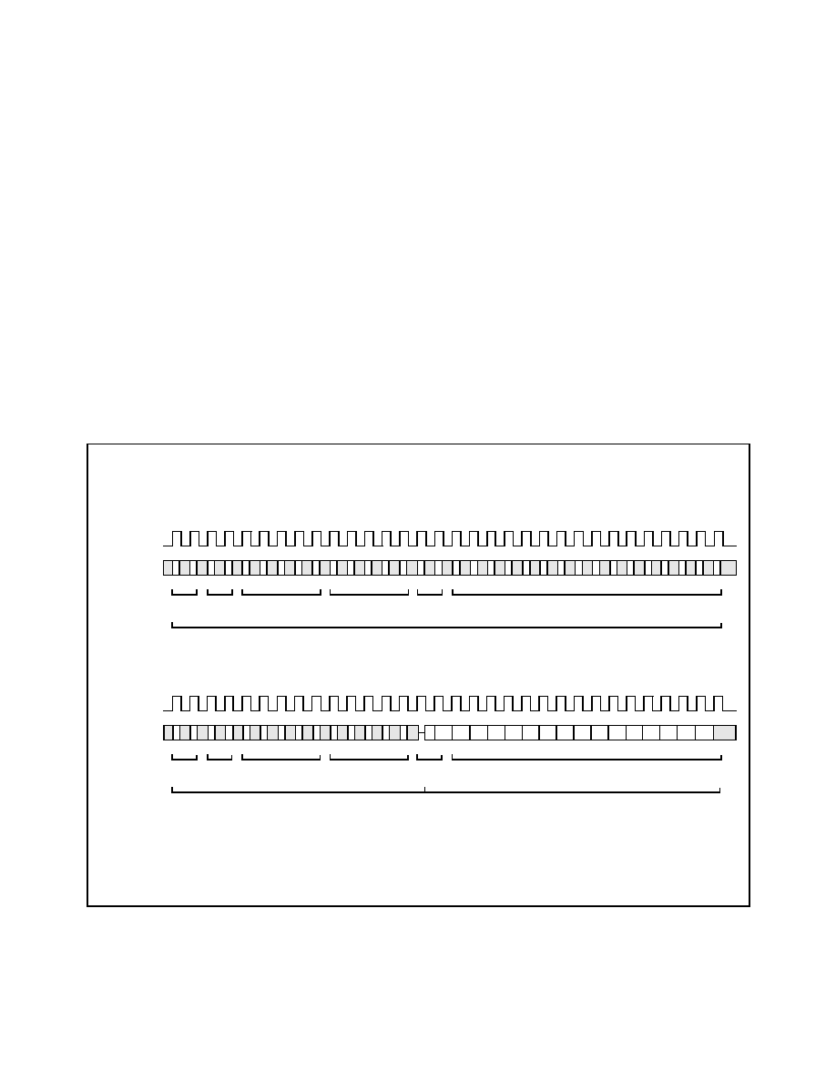
SMSC DS ≠ LAN83C183
75
Rev. 12/14/2000
4.2 GENERAL OPERATION
The MI serial port is idle when at least 32 continuous ones are detected on the bi-
directional MDIO data pin and remains idle as long as continuous ones are detected.
During idle, the MDIO output driver is in the high-impedance state. When the MI
serial port is in the idle state, a 0b01 pattern on the MDIO pin initiates a serial shift
cycle. Control and address bits are clocked into MDIO on the next 14 rising edges
of MDC (the MDIO output driver is still in a high-impedance state). If the multiple
register access mode is not enabled, data is either shifted in or out on MDIO on the
next 16 rising edges of MDC, depending on whether a write or read cycle was
selected with the READ and WRITE operation bits. After the 32 MDC cycles have
been completed:
∑
One complete register has been read or written
∑
The serial shift process is halted
∑
Data is latched into the device
∑
The MDIO output driver goes into a high-impedance state.
Another serial shift cycle cannot be initiated until the idle condition is detected again
(at least 32 continuous ones).
Figure 4.1
shows a timing diagram for a MI serial port
cycle.
Figure 4.1 MI Serial Port Frame Timing Diagram
4.3 MULTIPLE REGISTER ACCESS
Multiple registers can be accessed on a single MI serial port access cycle with the
multiple register access feature. Setting the Multiple Register Access Enable (MREG)
WRITE Cycle
MDC
MDIO
0
1
2
3
4
5
6
7
8
9
10
11
12
13
14
15
16
17
18
19
20
21
22
23
24
25
26
27
28
29
30
31
0
1
0
1
ST
OP
P4
P3
PHYAD
P2
P1
P0
R4
R3
REGAD
R2
R1
R0
1
0
TA
D15 D14 D13 D12 D11
DATA
D10 D9
D8
D7
D6
D5
D4
D3
D2
D1
D0
WRITE Bits
PHY clocks in data on rising edges of MDC with t
s
= 10 ns minimum and t
h
= 10 ns minimum
READ Cycle
MDC
MDIO
0
1
2
3
4
5
6
7
8
9
10
11
12
13
14
15
16
17
18
19
20
21
22
23
24
25
26
27
28
29
30
31
0
1
1
0
ST
OP
P4
P3
PHYAD
P2
P1
P0
R4
R3
REGAD
R2
R1
R0
Z
0
TA
D15 D14 D13 D12 D11
DATA
D10
D9
D8
D7
D6
D5
D4
D3
D2
D1
D0
WRITE Bits
PHY clocks in data on rising edges of MDC with
READ Bits
PHY clocks out data on rising edges of MDC with
t
s
= 10 ns minimum, and t
h
= 10 ns minimum
t
d
= 20 ns maximum
Note: ST = start bits, OP = operation bits (read or write), PHAD = PHY address, REGAD = register address, TA = turnaround bits
For more detailed timing information on t
h
,
t
h
,
and
t
h
, see Chapter 6, "Specifications."

SMSC DS ≠ LAN83C183
76
Rev. 12/14/2000
bit in the MI serial port Configuration 2 Register enables the multiple register access
feature.
When the PHYAD[4:0] bits in the MI frame match MDA[4:0]n pins on the device and
the REGAD[4:0] bits are set to 0b11111 during the first 16 clock cycles, all 11
registers are accessed on the 176 rising edges of MDC (11 registers x 16 bits per
register) that occur after the first 16 MDC clock cycles of the MI serial port access
cycle. There is no actual register residing at 0b1111, but this condition triggers the
access of multiple registers.
The registers (0, 1, 2, 3, 4, 5, 16, 17, 18, 19, and 20) are accessed in numerical
order from 0 to 20. After all 192 MDC clocks (16 + 176) have been completed:
∑
All the registers have been read or written
∑
The serial shift process is halted
∑
Data is latched into the device
∑
MDIO goes into a high-impedance state.
Another serial shift cycle cannot be initiated until the idle condition (at least 32
continuous ones) is detected.

SMSC DS ≠ LAN83C183
77
Rev. 12/14/2000
4.4 FRAME STRUCTURE
The structure of the serial port frame is shown in
Figure 4.2
and a timing diagram is
shown in
Figure 4.1
. Each serial port access cycle consists of 32 bits, exclusive of
idle. The first 16 bits of the serial port cycle are always write bits and are used for
control and addressing. The last 16 bits are data that is written to or read from a data
register.
The first two bits in
Figure 4.2
and
Figure 4.1
are start bits (ST[1:0]) and must be
written as a 0b01 for the serial port cycle to continue. The next two bits are the READ
and WRITE bits, which determine whether a registers is being read or written. The
next five bits are the PHY device address bits (PHYAD[4:0]), and they must match
the inverted values latched from the MDA[4:0]n pins during the power on reset time
for access to continue.
The next five bits are register address select (REGAD[4:0]) bits, which select one of
the 11 registers for access. The next two bits are turnaround (TA) bits, which are not
actual register bits but provide the device extra time to switch the MDIO pin function
from a write pin to a read pin, if necessary. The final 16 bits of the MI serial port cycle
are written to or read from the specific data register that the register address bits
(REGAD[4:0]) designate.
Figure 4.2
shows the MI frame structure.
IDLE Idle
Pattern
W
These bits are an idle pattern. The device does not
initiate an MI cycle until it detects an idle pattern of at least 32 con-
secutive ones.
ST[1:0]
Start Bits
W
When ST[1:0] = 01, a MI serial port access cycle starts.
READ
Read Select
W
When the READ bit is 1, it designates a read cycle.
WRITE
Write Select
W
When the WRITE bit is 1, it designates a write cycle.
PHYAD[4:0]
Physical Device Address
W
When the PHYAD[4:0] bits match the inverted latched value of the
MDA[3:0]n pins, the device's MI serial port is selected for operation.
REGAD[4:0]
Register Address
W
The REGAD[4:0] bits determine the specific register to access.
TA[1:0]
Turnaround Time
R/W
These bits provide some turnaround time for MDIO to allow it to
switch to a write input or read output, as needed. When READ = 1,
TA[1:0] = 0bZ0; when
WRITE = 1, TA[1:0] = 0b10.
D[15:0]
Data
R or W
These 16 bits contain data to or from one of the registers selected
with the register address bits REGAD[4:0].
Figure 4.2 MI Serial Frame Structure
IDLE
ST[1:0]
READ
WRITE
PHYAD[4:0]
REGAD[4:0]
TA[1:0]
D[15:0]

SMSC DS ≠ LAN83C183
78
Rev. 12/14/2000
4.5 REGISTER STRUCTURE
The device has 11 16-bit registers. A map of the registers is shown in
Section 3.2,
"MI Serial Port Register Summary"
. See
Chapter 3, Registers
for a complete
description of each register.
The 11 registers consist of six registers that are defined by IEEE 802.3 specifications
(registers 0 to 5) and five registers that are unique to the device (registers 16 through
20).
Table 4.1
gives a summary of the functions of each register.
Table 4.1 MI Serial Port Register Summary
Register
Name
Description
0
Control Register
Stores various configuration bits
1
Status Register
Contains device capability and status output bits
2
PHY ID 1
Contain an identification code unique to the device
3
PHY ID 2
4
AutoNegotiation
Advertisement
Contains bits that control the operation of the
AutoNegotiation algorithm
5
AutoNegotiation
Remote End
Capability
Contains bits that reflect the AutoNegotiation capabilities
of the link partner's PHY
16
Configuration 1
Stores various configuration bits
17
Configuration 2
Stores various configuration bits
18
Channel Status Output Contains status
19
Mask
Contains interrupt mask bits
20
Reserved
Reserved for factory use
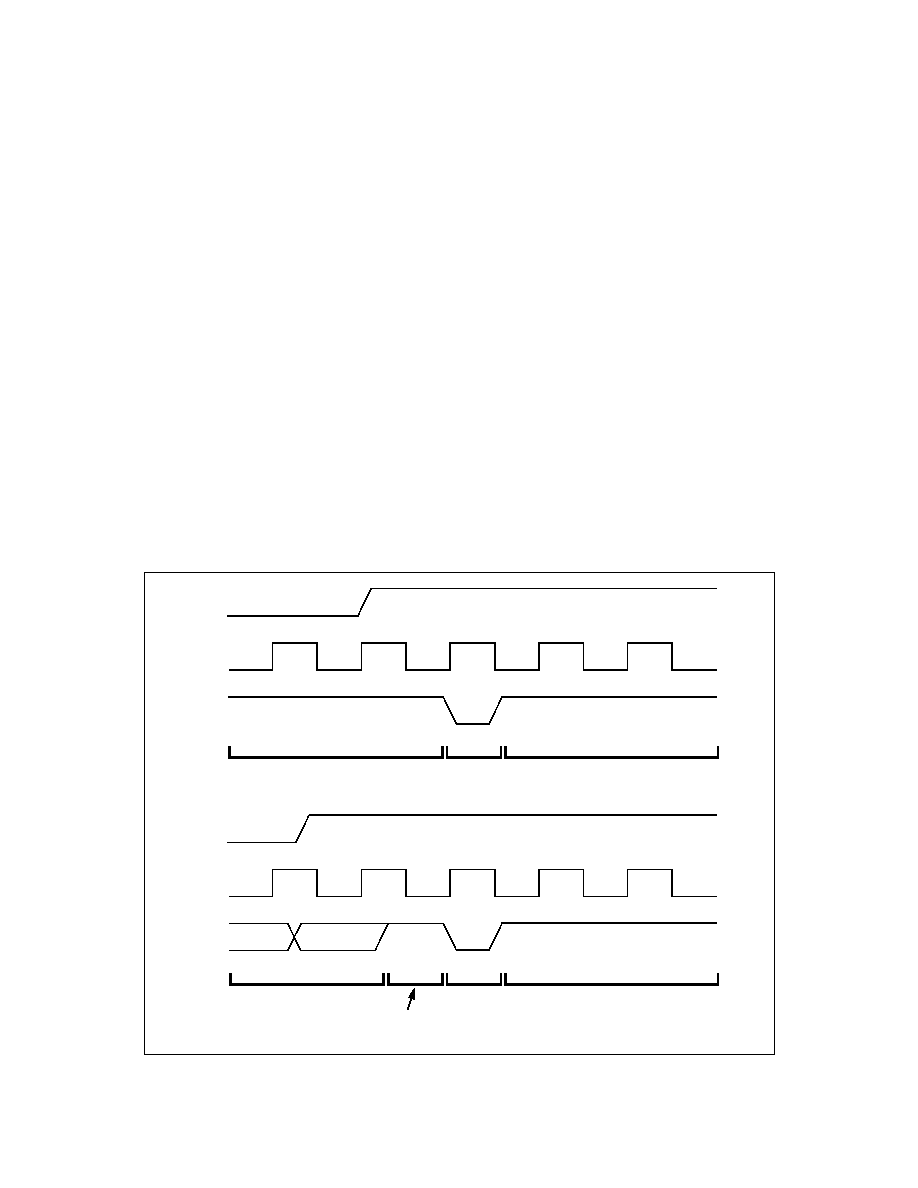
SMSC DS ≠ LAN83C183
79
Rev. 12/14/2000
4.6 INTERRUPTS
The device has hardware and software interrupt capability. Certain output status bits
(also referred to as interrupt bits) in the serial port trigger interrupts.
The R/LT interrupt bits (bits [14:6]) in the Channel Status Output Register cause an
interrupt when they transition provided they are not masked with the mask bits in the
Interrupt Mask register. These interrupt bits stay latched until read. When all interrupt
bits are read, the interrupt indication is removed and the interrupt bits that caused
the interrupt are updated to their current value.
Setting the appropriate mask register bits in the Interrupt Mask Register individually
can mask and remove an interrupt bit as a source of interrupt.
Interrupt indication is done in three ways:
∑
MDINTn pin: The MDINTn pin is an active-LOW interrupt output indication.
∑
INT bit: The INT bit in the Status Output Register, when set, indicates that one
or more interrupt bits have changed since the register was last read.
∑
Interrupt pulse on MDIO: When the Interrupt Scheme Select bit (INT_MDIO) is
set in the Configuration 2 register, an interrupt is indicated with a low-going pulse
on MDIO when MDC is high and the serial port is in the idle state, as shown in
the timing diagram in
Figure 4.3
. After the interrupt pulse, MDIO goes back to
the high-impedance state. If the interrupt occurs while the serial port is being
accessed, the MDIO interrupt pulse is delayed until one clock bit after the serial
port access cycle has ended, as shown in
Figure 4.3
Figure 4.3 MDIO Interrupt Pulse
INTERNAL
INTERRUPT
MDC
MDIO
MDIO HI-Z
Pulled High Externally
Interrupt
Pulse
MDIO HI-Z
Pulled High Externally
INTERNAL
INTERRUPT
MDC
MDIO
MDIO HI-Z
Pulled High Externally
Interrupt
Pulse
MDIO HI-Z
Pulled High Externally
B1
B0
Last Two Bits
of Read Cycle

SMSC DS ≠ LAN83C183
80
Rev. 12/14/2000

SMSC DS ≠ LAN83C183
81
Rev. 12/14/2000
Chapter 5
Specifications
This chapter contains the complete electrical, timing, and mechanical specifications
for the device. It contains the following sections:
∑
Section 5.1, "Absolute Maximum Ratings"
∑
Section 5.2, "Electrical Characteristics"
∑
Section 5.2.2, "FX Characteristics, Transmit"
∑
Section 5.3, "AC Electrical Characteristics"
∑
Section 5.4, "LED Driver Timing Characteristics"
∑
Section 5.5, "Pinouts and Package Drawings"
∑
Section 5.6, "Mechanical Drawing"

SMSC DS ≠ LAN83C183
82
Rev. 12/14/2000
5.1 ABSOLUTE MAXIMUM RATINGS
Table 5.1
shows the device absolute maximum ratings. These are limits which, if
exceeded, could cause permanent damage to the device or affect device reliability.
All voltages are specified with respect to GND unless otherwise specified.
Table 5.1 Absolute Maximum Ratings
Parameter
Range
Units
V
DD
Supply Voltage
-
0.3V to +4.0V
V
All Inputs and Outputs
-
0.3V to 5.5V
V
Package Power Dissipation
2.0 @ 70∞C
W
Storage Temperature
-
65 to +150
∞C
Temperature Under Bias
-
10 to +80 ∞C
∞C
Lead Temperature (soldering, 10 sec)
260
∞C
Body Temperature (soldering, 30 sec)
220
∞C

SMSC DS ≠ LAN83C183
83
Rev. 12/14/2000
5.2 ELECTRICAL CHARACTERISTICS
Table 5.2
lists the device DC electrical characteristics. Unless otherwise noted, all
test conditions are as follows:
TA = 0 to + 70 ∞C
V
DD
= 3.3 V ±5%
Clock = 25 MHz + 0.01%
REXT = 10 K
± 1%, no load
Table 5.2 DC Characteristics
Limit
Sym
Parameter Min
Typ
Max
Unit
Conditions
VIL
Input Low Voltage
0.8
Volt
All except OSCIN, MDA[4:0]n SD/FXDISn,
SD_THR
V
DD
-
1.0
Volt
MDA[4:0]n
1.5
Volt
OSCIN
0.45
Volt
SD/FXDISn (for FX disable), SD_THR (for
3.3V/5V select)
VIH
Input High Voltage
2
Volt
All except OSCIN, MDAn[4:0], SD/FXDISn,
SD_THR
V
DD
-
0.5
Volt
MDA[4:0]n
2.3
Volt
OSCIN
0.85
Volt
SD/FXDISn (for FX disable), SD_THR (for
3.3 V/5 V select)
IIL
Input Low Current
-
1
uA
VIN = GND All except OSCIN, MDA[4:0]n,
RESETn
-
4
-
25
uA
VIN = GND. MDA[4:0]n
-
12
-
120
uA
VIN = GND. RESETn
-
150
uA
VIN = GND. OSCIN
IIH
Input High Current
1
uA
VIN = V
DD
. All except OSCIN, RPTR
12
120
uA
VIN = V
DD
. RPTR
150
uA
VIN = V
DD
. OSCIN
VOL
Output Low
Voltage
0.4
Volt
IOL =
-
4 mA.
All except PLED[5:0]n
1
Volt
IOL =
-
10 mA. PLED[5:0]n
VOH
Output High
Voltage
V
DD
-
1.0
Volt
IOH = 4 mA. All Except PLED[5:0]n,
MDINTn
2.4
Volt
IOH = 4 uA.
PLED[5:2n], MDINTn
V
DD
-
1.0
Volt
IOH = 10 mA. PLED[1:0]n
CIN
Input Capacitance
5
pF

SMSC DS ≠ LAN83C183
84
Rev. 12/14/2000
5.2.1 Twisted-Pair DC Characteristics
Unless otherwise noted, all test conditions for TP transmit and receive operations are
as follows:
TA = 0 to + 70 ∞C
V
DD
= 3.3 V ± 5%
Clock = 25 MHz ±0.01%
REXT = 10 K
±1%, no load
TPO+/- loading is as shown in ?Application Note? or equivalent
62.5/10 MHz Square Wave on TP+/- inputs in 100/10 Mbits/s modes
Table 5.3
shows the twisted-pair characteristics for transmit operation.
I
DD
V
DD
Supply
Current
120
mA
Transmitting, 100 Mbits/s
140
mA
Transmitting, 10 Mbits/s
IGND
GND Supply
Current
190
mA
Transmitting, 100 Mbits/s
1
220
mA
Transmitting, 10 Mbits/s
1
IPDN
Powerdown
Supply Current
200
µ
A
Powerdown, either I
DD
or IGND
1. IGND includes current flowing into GND from the external resistors and transformer on TPO/FXO as shown in
?Application Note?
Table 5.2 DC Characteristics (Cont.)
Limit
Sym
Parameter Min
Typ
Max
Unit
Conditions
Table 5.3 Twisted Pair Characteristics (Transmit )
Sym
Parameter
Limit
Unit
Conditions
Min
Typ
Max
TOV
TP Differential Output
Voltage
0.950
1.000
1.050
V pk 100 Mbits/s, UTP Mode, 100 Ohm
Load
1.165
1.225
1.285
V pk 100 Mbits/s, STP Mode, 150 Ohm
Load
2.2
2.5
2.8
V pk 10 Mbits/s, UTP Mode, 100 Ohm
Load
2.694
3.062
3.429
V pk 10 Mbits/s, STP Mode, 150 Ohm
Load
TOVS
TP Differential Output
Voltage Symmetry
98
102
%
100 Mbits/s, ratio of positive and
negative amplitude peaks on TPO
±
TORF
TP Differential Output
Rise and Fall Time
3.0
5.0
nS
100 Mbits/s
TRF[1:0] = 0b10
TORFS
TP Differential Output
Rise and Fall Time
Symmetry
±
0.5
nS 100 Mbits/s, difference between rise
and fall times on TPO
±

SMSC DS ≠ LAN83C183
85
Rev. 12/14/2000
TODC
TP Differential Output
Duty Cycle Distortion
±
0.25
nS 100 Mbits/s, output data = 0101...
NRZ pattern unscrambled, measure
at 50% Points
TOJ
TP Differential Output
Jitter
±
1.4
nS 100 Mbits/s, output data = scrambled
/H/
TOO
TP Differential Output
Overshoot
5.0
%
100 Mbits/s
TOVT
TP Differential Output
Voltage Template
See
Figure 1.4
10 Mbits/s
TSOI
TP Differential Output
SOI Voltage Template
See
Figure 1.8
10 Mbits/s
TLPT
TP Differential Output
Link Pulse Voltage
Template
See
Figure 1.6
10 Mbits/s, NLP and FLP
TOIV
TP Differential Output
Idle Voltage
±
50
mV 10 Mbits/s. Measured on secondary
side of transformer in ?Apnote?.
TOIA
TP Output Current
38
40
42
mA pk 100 Mbits/s, UTP with TLVL[3:0] =
0b1000
31.06
32.66
34.26
mA pk 100 Mbits/s, STP with TLVL[3:0] =
0b1000
88
100
112
mA pk 10 Mbits/s, UTP with TLVL[3:0] =
0b1000
71.86
81.64
91.44
mA pk 10 Mbits/s, STP with TLVL[3:0] =
0b1000
TOIR
TP Output Current
Adjustment Range
0.80
1.2
VDD = 3.3 V, adjustable with REXT,
relative to TOIA with REXT = 10K
0.86
1.16
VDD = 3.3 V, Adjustable with
TLVL[3:0] See ?Application Note?,
relative to value at TLVL[3:0] =
0b1000
TORA
TP Output Current TLVL
Step Accuracy
±
50
% Relative to ideal values in
Figure 1.6
.
Table 1.6
values relative to output
with TLVL[3:0] = 0b1000.
TOR
TP Output Resistance
10 K
Ohm
TOC
TP Output Capacitance
15
pF
Table 5.3 Twisted Pair Characteristics (Transmit (Cont.) )
Sym
Parameter
Limit
Unit
Conditions
Min
Typ
Max

SMSC DS ≠ LAN83C183
86
Rev. 12/14/2000
Table 5.4
shows the twisted-pair characteristics for receive operation.
Table 5.4 Twisted Pair Characteristics (Receive )
Sym
Parameter
Limit
Unit
Conditions
Min
Typ
Max
RST
TP Input Squelch Threshold
166
500 mV pk 100 Mbits/s, RLVL0 = 0
310
540 mV pk 10 Mbits/s, RLVL0 = 0
60
200
mV pk 100 Mbits/s, RLVL0 = 1
186
324
mV pk 10 Mbits/s, RLVL0 = 1
RUT
TP Input Unsquelch
Threshold
100
300
mV pk 100 Mbits/s, RLVL0 = 0
186
324
mV pk 10 Mbits/s, RLVL0 = 0
20
90
mV pk 100 Mbits/s, RLVL0 = 1
112
194
mV pk 10 Mbits/s, RLVL0 = 1
ROCV TP Input Open Circuit
Voltage
VDD
- 2.4
±
0.2
Volt
Voltage on either TPI+ or TPI
-
with
respect to GND.
RCMR TP Input Common Mode
Voltage Range
ROCV
±
0.25
Volt
Voltage on TPI± with respect to
GND.
RDR
TP Input Differential Voltage
Range
VDD
Volt
RIR
TP Input Resistance
5 K
Ohm
RIC
TP Input Capacitance
10
pF

SMSC DS ≠ LAN83C183
87
Rev. 12/14/2000
5.2.2 FX Characteristics, Transmit
Unless otherwise noted, all test conditions for FX transmit and receive operations are
as follows:
∑
TA = 0 to +70 ∞C
∑
VDD=3.3 V
±
5%
∑
25 MHz
±
0.01%
∑
REXT=10 K
±
1%, no load
∑
FXO
±
Loading as shown in ?Apnote? or Equivalent
∑
125 MHz Square Wave on FXI+/- and SD Inputs
Table 5.5
shows the FX characteristics for transmit operation.
Table 5.5 FX Characteristics, Transmit
Sym
Parameter
Limit
Unit
Conditions
Min
Typ
Max
FOVH
FXO± Output
Voltage, High
VDD -
1.020
VDD -
0.880
V
Single-ended, measure FXO± relative
to GND
FOVL
FXO± Output
Voltage, Low
VDD -
1.810
VDD -
1.620
V
Single-ended, measure FXO± relative
to GND
FOIA
FXO± Output
Current
12
20
mA pk
FOIR
FXO± Output
Current
Adjustment
Range
0.85
1.15
VDD = 3.3 V, adjustable with REXT,
relative to FOIA with REXT = 10 K
0.85
1.30
VDD = 3.3 V, adjustable With FLVL[1:0],
relative To value at FLVL[1:0] = 0b10
FORA
FXO± Output
Current TLVL
Step Accuracy
±0.50
%
Relative to ideal values In
Table 1.9
FORF
FXO±
Differential
Output Rise and
Fall Time
1.3
ns
FORFS
FXO±
Differential
Output and Fall
Time Symmetry
±0.5
ns
Difference between rise nd fall times on
FXO+
FODC
FXO±
Differential
Output Duty
Cycle Distortion
±0.25
ns
Output Data = 0101... pattern measure at
50% points
FOJ
FXO±
Differential
Output Jitter
±1.3
ns
Output data = /H/
FOR
FXO± Output
Resistance
10 K
Ohm
FOC
FXO± Output
Capacitance
10
pF

SMSC DS ≠ LAN83C183
88
Rev. 12/14/2000
Table 5.6
shows the FX characteristics for receive operation.
Table 5.6 FX Characteristics, Receive
Sym
Parameter
Limit
Unit
Conditions
Min
Typ
Max
FDIV
FXI±
Differential
Input Voltage
0.150
V pk
FCMR
FXI± Input
Common Mode
Voltage Range
1.35
VDD -
0.80
V
Voltage on Either FXI+ or FXI- with respect to
GND
FSDIH
SD/FXDISn
Input High
Voltage
VTRIP -
50mV
V
When SD/FXDISn is used as a Signal Detect
input, not as the FX disable input.
VTRIP = (VDD -1.3V) ± 10%.
FSDIL
SD/FXDISn
Input Low
Voltage
VTRIP -
50 mV
V
When SD/FXDISn is used as a Signal Detect
input, not as the FX disable input.
VTRIP = (VDD - 1.3V) ± 10%
FSDTHR
SD_THR Input
Voltage
VDD -
1.3V -
2%
VDD -
1.3V
VDD -
1.3V +
2%
V
When interfacing to 5 V fiber transceivers.
When interfacing to 3.3 V fiber transceivers,
SD_THR is tied to GND.
FIR
FXI±,
SD/FXDISn
Input
Resistance
5K
ohm
FIC
FX±
SD/FXDISn
Input
Capacitance
10
pF

SMSC DS ≠ LAN83C183
89
Rev. 12/14/2000
5.3 AC ELECTRICAL CHARACTERISTICS
Unless otherwise noted, all test conditions are as shown in
Table 5.7
.
Table 5.7 Test Conditions
Test Condition
Parameter
Value
Temperature
TA
0 to +70∞C
Voltage
V
DD
3.3V ± 5%
Clock Frequency
25 MHz ± 0.01%
External Resistor
REXT
10K ± 1%, no load
Input Conditions
(all inputs)
tr, tf
10 ns, 20-80% points
Output Loading
TPO±
Open-drain outputs
All other digital
outputs
Same as ?Apnote? or
equivalent
10 pF
1K pullup, 50 pF
25 pF
Measurement Points
TPO±, TPI±
All other inputs and
outputs
0.0 V during data, ± 0.3 V at
start/end of packet
1.4 V
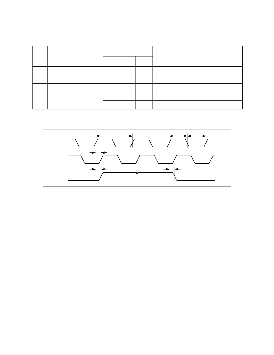
SMSC DS ≠ LAN83C183
90
Rev. 12/14/2000
5.3.1 25 MHz Input/Output Clock Timing Characteristics
Figure 5.1 25 MHz Output Timing
Table 5.8 25 MHz Input/Output Clock
1
Sym
Parameter
Limit
Unit
Conditions
Min
Typ
Max
t1
OSCIN Period
39.996
40 40.004
ns
Clock applied to OSCIN
t2
OSCIN High Time
16
ns
Clock applied to OSCIN
t3
OSCIN Low Time
16
ns
Clock applied to OSCIN
t4
OSCIN to TX_CLK Delay
10
ns
100 Mbits/s
20
ns
10 Mbits/s
1. Refer to
Figure 5.1
for Timing Diagram
OSCIN
t
1
t
2
t
3
TX_CLK
(100 Mbits/s)
t
4
t
4
t
4
TX_CLK
(10 Mbits/s)

SMSC DS ≠ LAN83C183
91
Rev. 12/14/2000
5.3.2 Transmit Timing Characteristics
Table 5.9
shows the Transmit AC timing parameters. See
Figure 5.2 and Figure 5.3
for the 100 Mbits/s and 10 Mbits/s transmit timing diagrams.
Table 5.9 Transmit Timing
Sym
Parameter
Limit
Unit
Conditions
Min
Typ
Max
t11
TX_CLK Period
39.996
40
40.004
ns
100 Mbits/s
399.96
400
400.04
ns
10 Mbits/s
t12
TX_CLK Low Time
16
20
24
ns
100 Mbits/s
160
200
240
ns
10 Mbits/s
t13
TX_CLK High Time
16
20
24
ns
100 Mbits/s
160
200
240
ns
10 Mbits/s
t14
TX_CLK Rise/Fall Time
10
ns
t15
TX_EN Setup Time
15
ns
Note
1
1. Setup time measured with 5 pF loading on TXC. Additional leading will create a delay on TXC rise time, which
requires increased setup times.
t16
TX_EN Hold Time
0
ns
t17
CRS During Transmit Assert Time
40
ns
100 Mbits/s
400
ns
10 Mbits/s
t18
CRS During Transmit Deassert
Time
160
ns
100 Mbits/s
900
ns
10 Mbits/s
t19
TXD Setup Time
15
ns
Note 1
t20
TXD Hold Time
0
ns
t21
TX_ER Setup Time
15
ns
Note 1
t22
TX_ER Hold Time
0
ns
t23
Transmit Propagation Delay
60
140
ns
100 Mbits/s, MII
140
ns
100 Mbits/s, FBI
600
ns
10 Mbits/s
t24
Transmit Output Jitter
± 0.7 ns pk-pk 100 Mbits/s
± 5.5
ns pk-pk 10 Mbits/s
t25
Transmit SOI Pulse Width To 0.3 V
250
ns
10 Mbits/s
t26
Transmit SOI Pulse Width to 40 mV
4500
ns
10 Mbits/s
t27
PLEDn Delay Time
25
ms
PLEDn programmed
for activity
t28
PLEDn Pulse Width
80
105
ms
PLEDn programmed
for activity
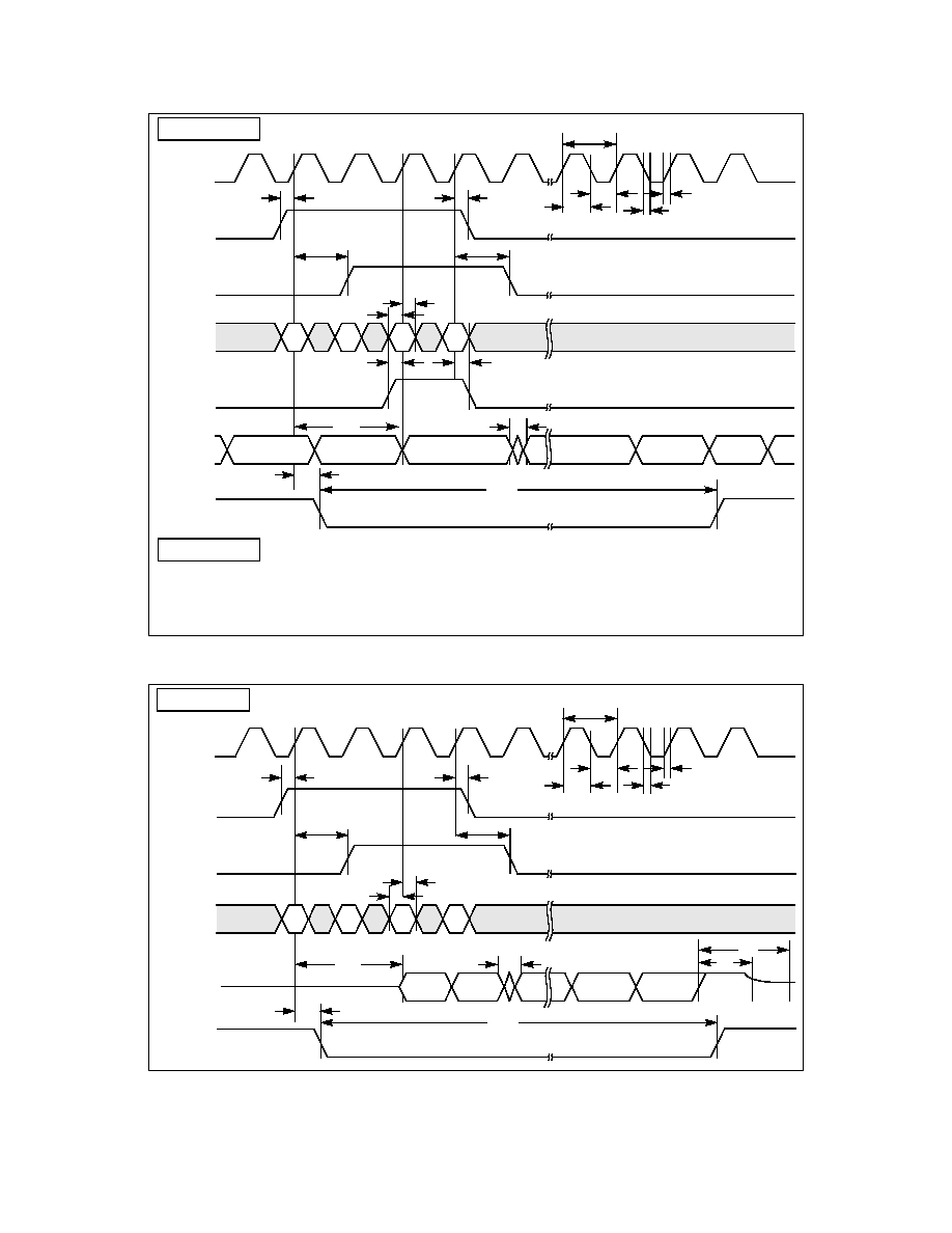
SMSC DS ≠ LAN83C183
92
Rev. 12/14/2000
Figure 5.2 Transmit Timing - 100 Mbits/s
Figure 5.3 Transmit Timing - 10 Mbits/s
N1
TX_CLK
TX_EN
TXD[3:0]
TPO±
N0
N2
t
15
t
19
t
27
t
28
t
11
t
16
PLEDn
IDLE
IDLE
/J/K/
DATA
/T/R/
IDLE
t
23
t
24
CRS
t
13
t
12
t
14
t
14
t
18
t
17
N3
t
20
t
22
t
21
TX_ER
MII 100 Mbits/s
FBI 100 Mbits/s
Same as MII 100 Mbits Except:
1. TX_ER Converted to TXD4
2. RX_ER Converted to RXD4
PREAMBLE
PREAMBLE
DATA
SOI
DATA
N1
TX_CLK
TX_EN
TXD[3:0]
TP0±
N0
N2
t
15
t
19
t
27
t
28
t
11
t
16
PLEDn
t
23
CRS
t
13
t
12
t
14
t
14
t
18
t
17
N3
t
20
t
24
t
26
t
25
MII 10 Mbits/s

SMSC DS ≠ LAN83C183
93
Rev. 12/14/2000
5.3.3 Receive Timing Characteristics
Table 5.10
shows the Receive AC timing parameters. See
Figure 5.4
through
Figure
5.8
for the receive timing diagrams.
Table 5.10 Receive Timing
Limit
Sym
Parameter
Min
Typ
Max
Unit
Conditions
t31
Start Of Packet To
CRS
Assert Delay
200
ns
100 Mbits/s, MII
200
ns
100 Mbits/s, FBI
700
ns
10 Mbits/s
t32
End Of Packet To
CRS
Deassert Delay
130
240
ns
100 Mbits/s, MII
240
ns
100 Mbits/s, FBI
600
ns
10 Mbits/s. relative to start of SOI pulse
t33
Start Of Packet To
RX_DV Assert
Delay
240
ns
100 Mbits/s
3600
ns
10 Mbits/s
t34
End Of Packet To
RX_DV Deassert
Delay
280
ns
100 Mbits/s
1000
ns
10 Mbits/s. relative to start of SOI pulse
t37 RX_CLK
To
RX_DV,
RXD, RX_ER
Delay
-
8
8
ns
100 Mbits/s
-
80 80
ns
10
Mbits/s
t38
RX_CLK High
Time
18 20
22
ns
100
Mbits/s
180
200
600
ns
10 Mbits/s
t39
RX_CLK Low Time
18
20
22
ns
100 Mbits/s
180 200
600
ns
10
Mbits/s
t40
SOI Pulse
Minimum Width
Required for Idle
Detection
125
200
ns
10 Mbits/s measure TPI
±
from last zero
cross to 0.3V point.
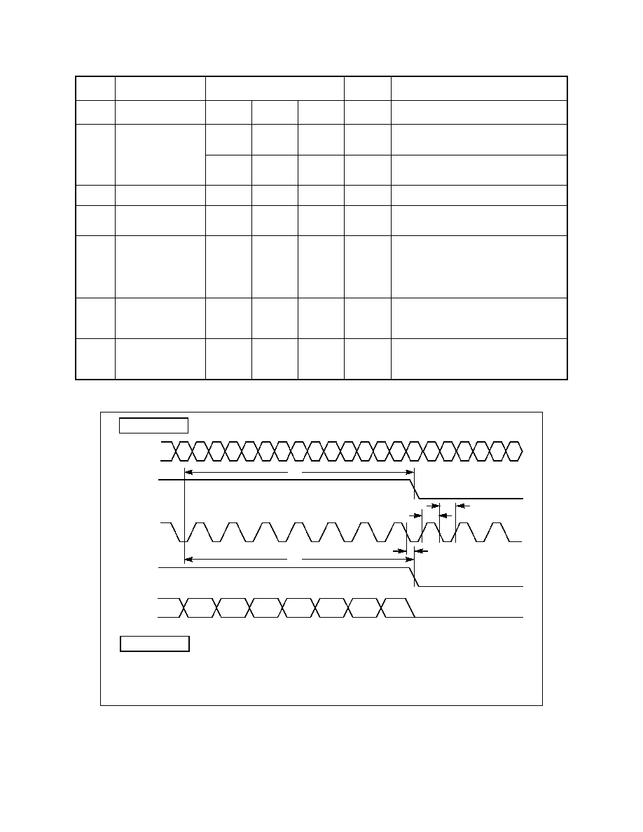
SMSC DS ≠ LAN83C183
94
Rev. 12/14/2000
Figure 5.4 Receive Timing, Start of Packet - 100 Mbits/s
t41
Receive Input Jitter
±3.0
ns pk -
pk
100 Mbits/s
±13.5
ns pk -
pk
10 Mbits/s
t43
PLEDn Delay Time
25
ms
PLEDn programmed for activity
t44
PLEDn Pulse
Width
80
105
ms
PLEDn programmed for activity
t45
RX_CLK, RXD,
CRC, RX_DV,
RX_ER Output
Rise and Fall
Times
10
ns
t46
RX_EN Deassert
to Rcv MII Output
HI-Z Delay
40
ns
t47
RX_EN Assert to
Rcv MII Output
Active Delay
40
ns
Table 5.10 Receive Timing (Cont.)
Limit
Sym
Parameter
Min
Typ
Max
Unit
Conditions
RX
RX
RX
RX
RX
RX
RX
RX
TX
TX
t
38
DATA
T
TPI
+/-
CRS
RX_CLK
RXD[3:0]
R
I
t
32
I
I
I
I
I
I
I
I
I
I
I
I
I
I
I
I
I
I
DATA
DATA
DATA
DATA
DATA
DATA
DATA
MII 100 Mbits/s
t
39
t
34
t
37
RX_DV
FBI 100 Mbits/s
Same as MII 100 Mbits Except:
1. TX_ER converted to RXD4
2. RX_ER converted to TXD4
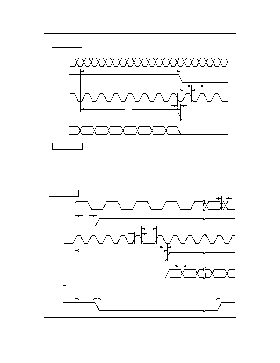
SMSC DS ≠ LAN83C183
95
Rev. 12/14/2000
Figure 5.5 Receive Timing, End of Packet - 100 Mbits/s
Figure 5.6 Receive Timing, Start of Packet - 10 Mbits/s
RX
RX
RX
RX
RX
RX
RX
RX
TX
TX
t
38
DATA
T
TPI
+/-
CRS
RX_CLK
RXD[3:0]
R
I
t
32
I
I
I
I
I
I
I
I
I
I
I
I
I
I
I
I
I
I
DATA
DATA
DATA
DATA
DATA
DATA
DATA
MII 100 Mbits/s
t
39
t
34
t
37
RX_DV
FBI 100 Mbits/s
Same as MII 100 Mbits Except:
1. TX_ER converted to RXD4
2. RX_ER converted to TXD4
RX
RX
RX
RX
RX
RX
TX
TX
TX
TX
TX
DATA
TPI
+/-
CRS
RX_CLK
RXD[3:0]
DATA
t
37
DATA
DATA
t
41
t
31
DATA
PREAMBLE
t
43
RX_ER
t
44
PREAMBLE
t
38
t
39
t
33
PLEDn
RX_DV
t
37
MII 10 Mbits/s
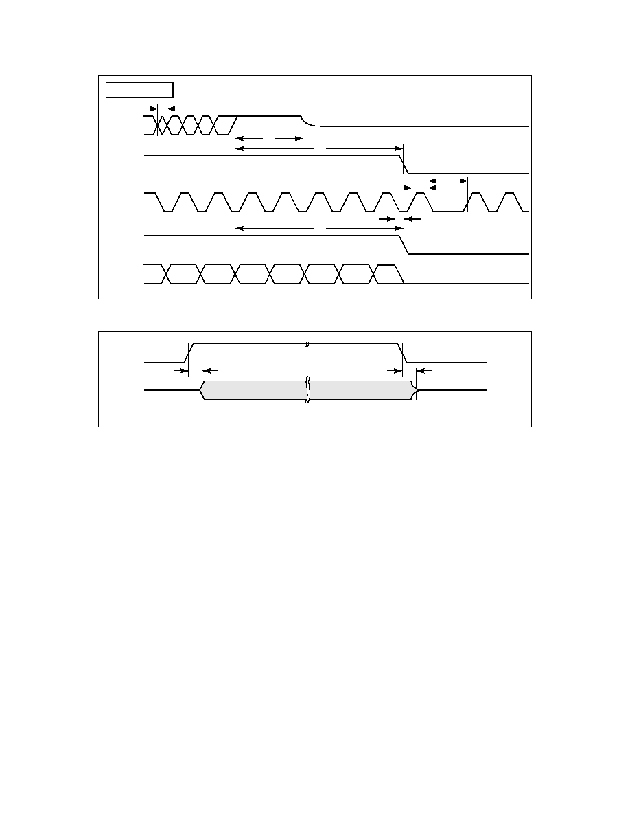
SMSC DS ≠ LAN83C183
96
Rev. 12/14/2000
Figure 5.7 Receive Timing, End of Packet - 10 Mbits/s
Figure 5.8 RX_EN Timing
TPI
+/-
CRS
RX_CLK
RX_DV
DATA
t
41
DATA
SOI
t
32
t
40
t
38
t
37
DATA
DATA
DATA
DATA
DATA
DATA
RX
RXD[3:0]
RX
RX
RX
RX
RX
RX
RX
TX
TX
t
39
t
34
DATA DATA
DATA
DATA
MII 10 Mbits/s
RX_EN
RX_CLK
RXD[3:0]
RX_DV
RX_ER
COL
t
47
t
46
SMSC DS ≠ LAN83C183
97
Rev. 12/14/2000
5.3.4 Collision and JAM Timing Characteristics
Table 5.11
shows the Collision and JAM timing parameters. See
Figure 5.9
through
Figure 5.14
for the associated timing diagrams.
Figure 5.9 Collision Timing, Receive 100 Mbits/s
Table 5.11 Collision and Jam Timing
LIMIT
SYM
PARAMETER
MIN
TYP
MAX
UNIT
CONDITIONS
t51
Rcv Packet Start To
COL Assert Time
200
ns 100 Mbits/s
700
ns 10 Mbits/s
t52
Rcv Packet Stop To
COL Deassert Time
130
240
ns
100 Mbits/s
300
ns 10 Mbits/s
t53
Xmt Packet Start To
COL Assert Time
200
ns 100 Mbits/s
700
ns 10 Mbits/s
t54
Xmt Packet Stop To
COL Deassert Time
240
ns 100 Mbits/s
300
ns 10 Mbits/s
t55
PLEDn Delay Time
25
ms PLEDn programmed for collision
t56 PLEDn Pulse Width
80
105
ms
PLEDn programmed for collision
t57
Collision Test Assert Time
5120
ns
t58
Collision Test Deassert Time
40
ns
t59
CRS Assert To Transmit
JAM Packet Start During JAM
300
ns 100 Mbits/s
800
ns 10 Mbits/s
t60
1
COL Rise And Fall Time
10
ns
1. Timing not shown
TPO
+/-
TPI
+/-
COL
PLEDn
MII 100 Mbits/s
I
DATA
DATA
DATA
DATA
DATA
DATA
DATA
DATA
DATA
DATA
DATA
DATA
DATA
I
I
I
I
J
K
DATA
DATA
DATA
DATA
T
R
I
I
t
51
t
52
t
56
t
55
FBI 100 Mbits/s
Same as MII 100 Mbits
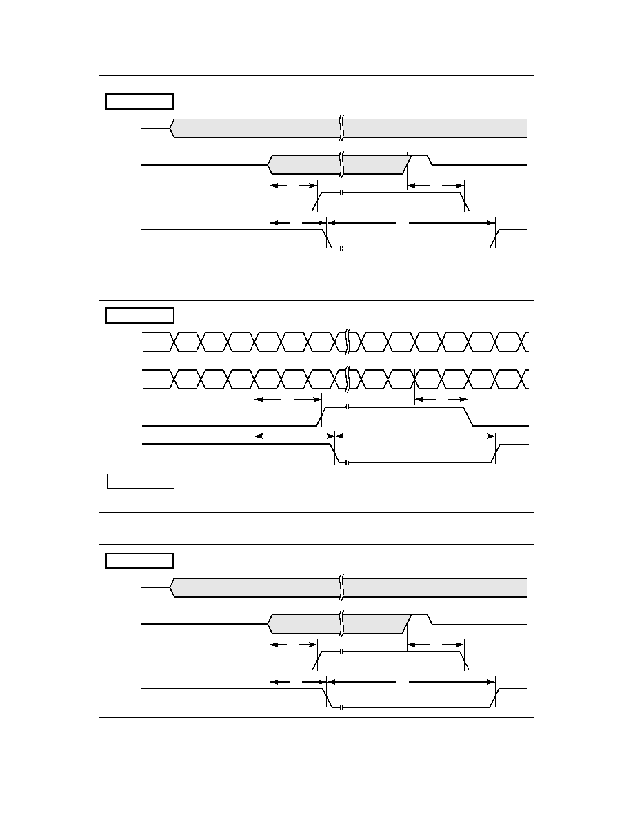
SMSC DS ≠ LAN83C183
98
Rev. 12/14/2000
Figure 5.10 Collision Timing, Receive 10 Mbits/s
Figure 5.11 Collision Timing, Transmit - 100 Mbits/s
Figure 5.12 Collision Timing, Transmit - 10 Mbits/s
MII 100 Mbits/s
t
51
t
52
t
55
t
56
TPO
+/-
TPI
+/-
COL
PLEDn
TPO
+/-
TPI
+/-
COL
PLEDn
MII 100 Mbits/s
I
DATA
DATA
DATA
DATA
DATA
DATA
DATA
DATA
DATA
DATA
DATA
DATA
DATA
I
I
I
I
J
K
DATA
DATA
DATA
DATA
T
R
I
I
t
53
t
54
t
56
t
55
Same as MII 100 Mbits
FBI 100 Mbits/s
MII 100 Mbits/s
t
53
t
54
t
55
t
56
TPI
+/-
TPO
+/-
COL
PLEDn
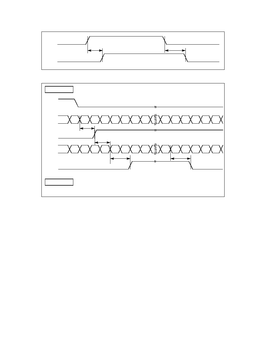
SMSC DS ≠ LAN83C183
99
Rev. 12/14/2000
Figure 5.13 Collision Test Timing
Figure 5.14 JAM Timing
COL
TX_EN
t
58
t
57
TPO
+/-
CRS
COL
MII 100 Mbits/s
I
I
J
DATA DATA
DATA
DATA DATA DATA
t
53
t
53
Same as MII 100 Mbits
FBI 100 Mbits/s
JAMn
K
DATA DATA
DATA
DATA DATA DATA
I
I
I
K
JAM
T
I
I
J
I
t
59
JAM
JAM
JAM
R
I
I
t
54
TPO
+/-

SMSC DS ≠ LAN83C183
100
Rev. 12/14/2000
5.3.5 Link Pulse Timing Characteristics
Table 5.12
shows the Link Pulse AC timing parameters. See
Figure 5.15
and
Figure
5.16
for the Link Pulse timing diagrams.
Table 5.12 Link Pulse Timing
Sym
Parameter
Limit
Unit
Condition
Min
Typ
Max
t61
NLP Transmit Link Pulse
Width
See
Figure 1.7
ns
t62
NLP Transmit Link Pulse
Period
8
24
ms
t63
NLP Receive Link Pulse
Width Required For
Detection
50
ns
t64
NLP Receive Link Pulse
Minimum Period Required
For Detection
6
7
ms
link_test_min
t65
NLP Receive Link Pulse
Maximum Period Required
For Detection
50
150 ms
link_test_max
t66
NLP Receive Link Pulses
Required To Exit Link Fail
State
3
3
3
Link
Pulses
lc_max
t67
FLP Transmit Link Pulse
Width
100
150 ns
t68
FLP Transmit Clock Pulse To
Data Pulse Period
55.5 62.5
69.5
µ
s
interval_timer
t69
FLP Transmit Clock Pulse To
Clock Pulse Period
111
125
139
µ
s
t70
FLP Transmit Link Pulse
Burst Period
8
22
ms
transmit_link_burst_timer
t71
FLP Receive Link Pulse
Width Required For
Detection
50
ns
t72
FLP Receive Link Pulse
Minimum Period Required
For Clock Pulse Detection
5
25
µ
s
flp_test_min_timer
t73
FLP Receive Link Pulse
Maximum Period Required
For Clock Pulse Detection
165
185
µ
s
flp_test_max_timer
t74
FLP Receive Link Pulse
Minimum Period Required
For Data Pulse Detection
15
47
µ
s
data_detect_min_
timer
t75
FLP Receive Link Pulse
Maximum Period Required
For Data Pulse Detection
78
100
µ
s
data_detect_max_
timer
SMSC DS ≠ LAN83C183
101
Rev. 12/14/2000
Figure 5.15 NLP Link Pulse Timing
t76
FLP Receive Link Pulses
Required To Detect Valid
FLP Burst
17
17
Link
Pulses
t77
FLP Receive Link Pulse
Burst Minimum Period
Required For Detection
5
7
ms
nlp_test_min_timer
t78
FLP Receive Link Pulse
Burst Maximum Period
Required For Detection
50
150
ms
nlp_test_max_
timer
t79
FLP Receive Link Pulses
Bursts Required To Detect
AutoNegotiation Capability
3
3
3
Link
Pulse
t80
FLP Receive Acknowledge
Fail Period
1200
1500
ms
t81
FLP Transmit Renegotiate
Link Fail Period
1200
1500
ms
break_link_timer
t82
NLP Receive Link Pulse
Maximum Period Required
For Detection After FLP
Negotiation Has Completed
750
1000
ms
link_fail_inhibit_
timer
Table 5.12 Link Pulse Timing (Cont.)
Sym
Parameter
Limit
Unit
Condition
Min
Typ
Max
TPO
+/-
TPI
+/-
PLEDn
a. Transmit NLP
b. Receive NLP
t
61
t
64
t
63
t
65
t
66
t
62
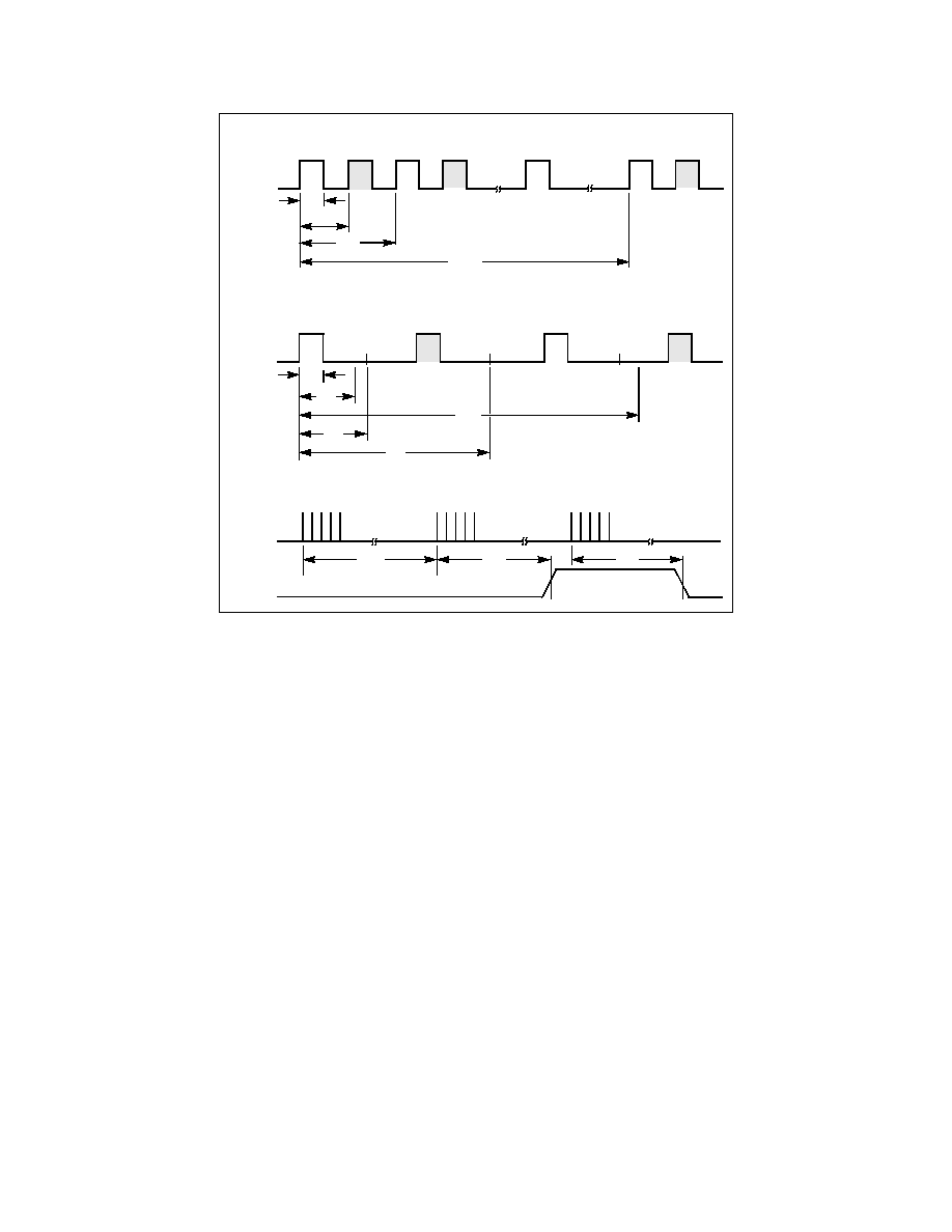
SMSC DS ≠ LAN83C183
102
Rev. 12/14/2000
Figure 5.16 FLP Link Pulse Timing
TPI
+/-
t
78
t
77
t
79
PLEDn
a. Transmit FLP and Transmit FLP Burst
CLK
DATA
CLK
DATA
CLK
DATA
CLK
TPO
+/-
t
68
t
69
t
67
t
70
CLK
DATA
CLK
DATA
t
73
t
71
31.25
62.50
125.00
156.25
t
74
t
75
TPI
+/-
b. Receive FLP
c. Receive FLP Burst
93.75
t
72
SMSC DS ≠ LAN83C183
103
Rev. 12/14/2000
5.3.6 Jabber Timing Characteristics
Table 5.13
shows the Jabber AC timing parameters. See
Figure 5.17
for the Jabber
timing diagram.
Figure 5.17 Jabber Timing
Table 5.13 Jabber Timing
Sym
Parameter
Limit
Unit
Conditions
Min
Typ
Max
t91
Jabber Activation Delay Time
50
100
ms 10 Mbits/s
t92
Jabber Deactivation Delay Time
250
750
ms
10 Mbits/s
TPO
+/-
TXEN
CRS
COL
t
91
t
92
t
91
t
91
FBI 100 Mbits/s
MI 10 Mbits/s
Not applicable
MII 100 Mbits/s
Not applicable
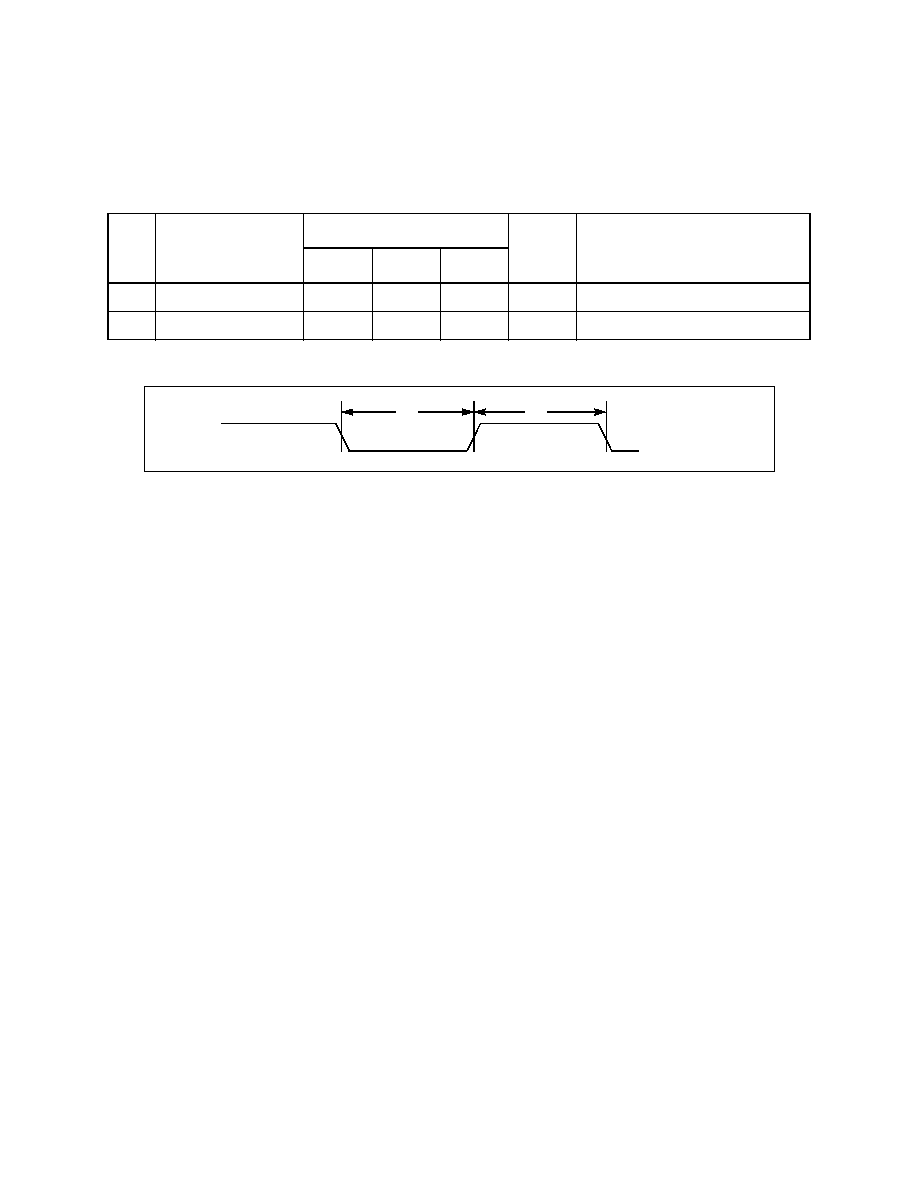
SMSC DS ≠ LAN83C183
104
Rev. 12/14/2000
5.4 LED DRIVER TIMING CHARACTERISTICS
Table 5.14
shows the Jabber AC timing parameters. See
Figure 5.18
for the Jabber
timing diagram.
Figure 5.18 LED Driver Timing
Table 5.14 LED Driver Timing
Sym
Parameter
Limit
Unit
Conditions
Min
Typ
Max
t96
PLED[5:0]n On Time
80
105
ms
PLED[5:0]n programmed to blink
t97
PLED[5:0]n Off Time
80
105
ms
PLED[5:0]n programmed to blink
PLED[5:0]n
t
96
t
97
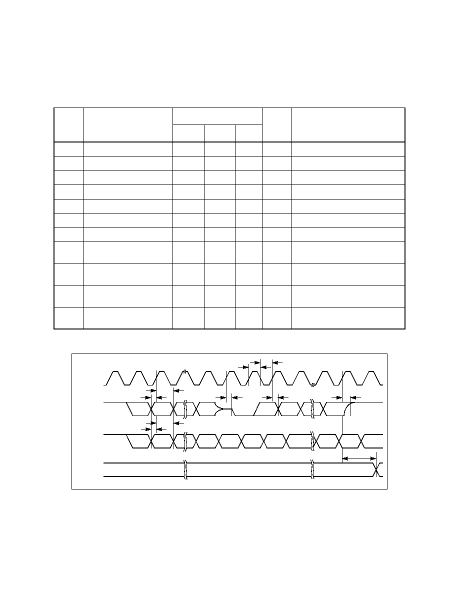
SMSC DS ≠ LAN83C183
105
Rev. 12/14/2000
5.4.1 MI Serial Port Timing Characteristics
Table 5.15
shows the MI Serial Port AC timing parameters. See
Figure 5.19
and
Figure 5.20
for the associated timing diagram.
Figure 5.19 MI Serial Port Timing
Table 5.15 MI Serial Port Timing
Sym
Parameter
Limit
Unit
Conditions
Min
Typ
Max
t101
MDC High Time
20
ns
t102
MDC Low Time
20
ns
t103
MDIO Setup Time
10
ns
Write bits
t104
MDIO Hold Time
10
ns
Write bits
t105
MDC To MDIO Delay
20
ns
Read bits
t106
MDIO Hi-Z To Active Delay
20
ns
Write-Read Bit Transition
t107
MDIO Active To HI-Z Delay
20
ns
Read-Write bit transition
t108
Frame Delimiter (Idle)
32
Clocks Number of consecutive MDC clocks
with MDIO = 1
t109
End Of Frame To MDINTn
Transition
100 ns
t110
MDC To MDIO Interrupt
Pulse Assert Delay
100 ns
t111
MDC To MDIO Interrupt
Pulse Deassert Delay
100 ns
MDIO
MDC
(READ)
MDIO
(WRITE)
0
ST1
ST0
REGAD0
TA1
TA0
D15
D1
D0
1
13
14
15
16
17
30
31
t
103
t
104
t
103
t
106
TA1
t
105
t
107
t
104
ST1
ST0
REGAD0
TA0
D15
D14
D0
t
101
t
102
MDINTn
t
109
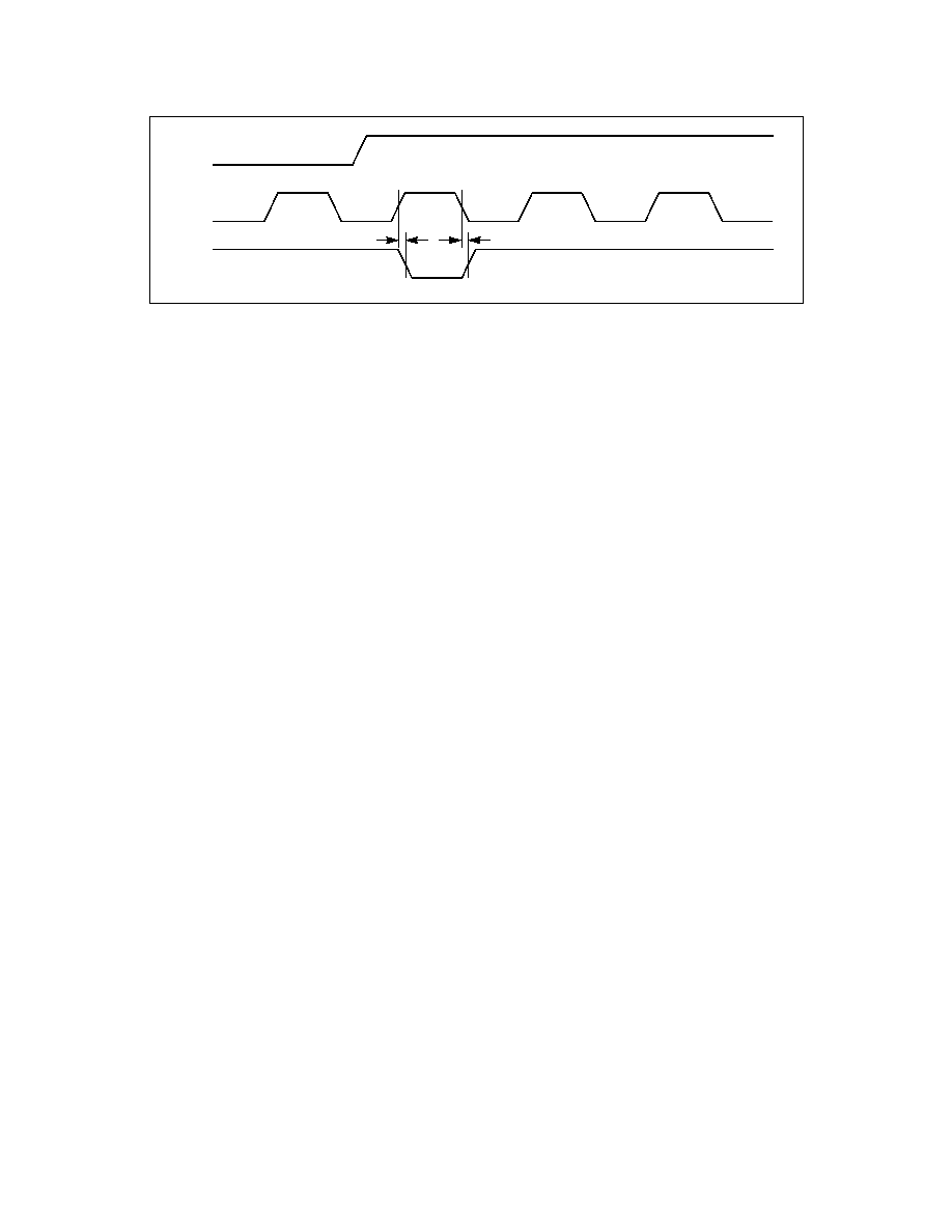
SMSC DS ≠ LAN83C183
106
Rev. 12/14/2000
Figure 5.20 MDIO Interrupt Pulse Timing
Internal
t
110
MDC
t
111
MDIO
Interrupt
Signal

SMSC DS ≠ LAN83C183
107
Rev. 12/14/2000
5.5 PINOUTS AND PACKAGE DRAWINGS
This section contains the alphabetical and numerical pin listings for the LAN83C183
as well as its pinouts and package drawing.
5.5.1 Pinouts
Table 5.16
and
Table 5.17
contain the list of LAN83C183 signals. The first table lists
the signals by category and the second lists them by pin number.
Table 5.16 LAN83C183 Pin List (by Signal Category)
Pin Name
Pin Number
Description
Media Interface
REXT
50
Transmit Current Set
SD/FXDISn
53
Signal Detect/FX Interface Disable
SD_THR
51
Signal Detect Input Threshold Level Set
TPI -/FXO+
59
Twisted Pair Receive Input, Negative/Fiber Pair Transmit Output, Positive
TPI+/FXO-
58
Twisted Pair Receive Input, Positive/Fiber Pair Transmit Output, Negative
TPO-/FXI+
55
Twisted Pair Transmit Output, Negative/Fiber Pair Transmit Input, Positive
TPO+/FXI-
54
Twisted Pair Transmit Output, Positive/Fiber Pair Transmit Input, Negative
Controller Interface
CRS
13
Carrier Sense Output
OSCIN
42
Clock Oscillator Input
RX_CLK
26
Receive Clock Output
RX_DV
14
Receive Data Valid Output
RX_EN/JAMn
27
Receive Enable Input/JAM Input
RX_ER/RXD4
18
Receive Error Output/Fifth Receive Data Bit Output
RXD0
22
Receive Data Output.
RXD1
21
Receive Data Output.
RXD2
20
Receive Data Output.
RXD3
19
Receive Data Output
TX_CLK
34
Transmit Clock Output
TX_EN
40
Transmit Enable Input
TX_ER/TXD4
39
Transmit Error Input/Fifth Transmit Data Bit Input
TXD0
35
Transmit Data Input.
TXD1
36
Transmit Data Input.
TXD2
37
Transmit Data Input.
TXD3
38
Transmit Data Input
Management Interface (MI)
MDC
10
Management Interface (MI) Clock Input
MDIO
11
Management Interface (MI) Data Input/Output
MDINTn/MDA4n
9
Management Interface (MI) Data Input/Output
PLED0n/MDA0n
61
Programmable LED Output /Management Interface Address Input.

SMSC DS ≠ LAN83C183
108
Rev. 12/14/2000
PLED1n/MDA1n
62
Programmable LED Output /Management Interface Address Input
PLED2n/MDA2n
3
Programmable LED Output /Management Interface Address Input
PLED3n/MDA3n
4
Programmable LED Output /Management Interface Address Input
PLED4n
2
Programmable LED Output
PLED5n
63
Programmable LED Output
Miscellaneous
ANEG 30
AutoNegotiation
Input
COL 12
Collision
Output
DPLX
29
Full/Half Duplex Select Input
RESETn
44
Reset Input
RPTR
24
Repeater Mode Enable Input
SPEED
28
Speed Select Input
Table 5.16 LAN83C183 Pin List (by Signal Category) (Cont.)
Pin Name
Pin Number
Description

SMSC DS ≠ LAN83C183
109
Rev. 12/14/2000
Power
V
DD
1
56
Positive Supply. 3.3V ± 5% Volts
V
DD
2
57
V
DD
3
7
V
DD
4
8
V
DD
5
25
V
DD
6
32
Ground
GND1
52
Ground
GND2
60
GND3
6
GND4
41
GND5
23
GND6
31
No Connection
NC
1
No Connection
NC
5
NC
15
NC
16
NC
17
NC
33
NC
43
NC
45
NC
46
NC
47
NC
49
NC
48
NC
64
Table 5.16 LAN83C183 Pin List (by Signal Category) (Cont.)
Pin Name
Pin Number
Description

SMSC DS ≠ LAN83C183
110
Rev. 12/14/2000
.
Table 5.17 LAN83C183 Pin List (by Pin Number)
Pin
Number
Pin Name
Description
1
NC
No Connection
2
PLED4n
Programmable LED Output
3
PLED2n/MDA2n
Programmable LED Output /Management Interface Address Input
4
PLED3n/MDA3n
Programmable LED Output /Management Interface Address Input
5
NC
No Connect
6
GND3
Ground
7
VDD3
Positive Supply. 3.3V ± 5% Volts
8
VDD4
Positive Supply. 3.3V ± 5% Volts
9
MDINTn/MDA4n
Management Interface (MI) Data Input/Output
10
MDC
Management Interface (MI) Clock Input
11
MDIO
Management Interface (MI) Data Input/Output
12
COL Collision
Output
13
CRS Carrier
Sense
Output
14
RX_DV
Receive Data Valid Output
15
NC
No Connect
16
NC
No Connect
17
NC
No Connect
18
RX_ER/RXD4
Receive Error Output/Fifth Receive Data Bit Output
19
RXD3 Receive
Data
Output
20
RXD2
Receive Data Output.
21
RXD1
Receive Data Output.
22
RXD0
Receive Data Output.
23
GND5
Ground
24
RPTR
Repeater Mode Enable Input
25
VDD5
Positive Supply. 3.3V ± 5% Volts
26
RX_CLK
Receive Clock Output
27
RX_EN/JAMn
Receive Enable Input
28
SPEED
Speed Select Input
29
DPLX
Full/Half Duplex Select Input
30
ANEG AutoNegotiation
Input
31
GND6
Ground
32
VDD6
Positive Supply. 3.3V ± 5% Volts
33
NC
No Connect
34
TX_CLK Transmit
Clock
Output
35
TXD0
Transmit Data Input.

SMSC DS ≠ LAN83C183
111
Rev. 12/14/2000
36
TXD1
Transmit Data Input.
37
TXD2
Transmit Data Input.
38
TXD3
Transmit Data Input
39
TX_ER/TXD4
Transmit Error Input/Fifth Transmit Data Bit Input
40
TX_EN
Transmit Enable Input
41
GND4
Ground
42
OSCIN
Clock Oscillator Input
43
NC
No Connect
44
RESETn
Reset Input
45
NC
No Connect
46
NC
No Connect
47
NC
No Connect
48
NC
No Connect
49
NC
No Connect
50
REXT
Transmit Current Set
51
SD_THR
Signal Detect Input Threshold Level Set
52
GND1
Ground
53
SD/FXDISn
Signal Detect/FX Interface Disable
54
TPO+/FXI-
Twisted Pair Transmit Output, Positive/Fiber Pair Transmit Input, Negative
55
TPO-/FXI+
Twisted Pair Transmit Output, Negative/Fiber Pair Transmit Input, Positive
56
VDD1
Positive Supply. 3.3V ± 5% Volts
57
VDD2
Positive Supply. 3.3V ± 5% Volts
58
TPI+/FXO-
Twisted Pair Receive Input, Positive/Fiber Pair Transmit Output, Negative
59
TPI -/FXO+
Twisted Pair Receive Input, Negative/Fiber Pair Transmit Output, Positive
60
GND2
Ground
61
PLED0n/MDA0n
Programmable LED Output /Management Interface Address Input.
62
PLED1n/MDA1n
Programmable LED Output /Management Interface Address Input
63
PLED5n
Programmable LED Output
64
NC
No Connect
Table 5.17 LAN83C183 Pin List (by Pin Number) (Cont.)
Pin
Number
Pin Name
Description
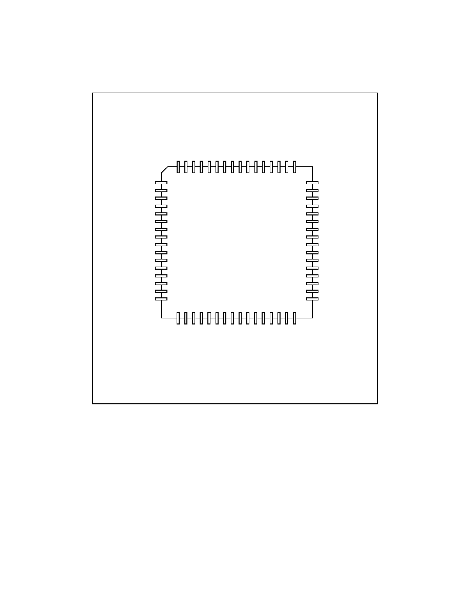
SMSC DS ≠ LAN83C183
112
Rev. 12/14/2000
5.5.2 LAN83C183 Pin Layout
Figure 5.21
shows the pin layout for the LAN83C183 package.
Figure 5.21 LAN83C183 64-Pin LQFP, Top View
LAN83C183
64-Pin LQFP
Top View
NC
PLED4n
PLED2n/MDA2n
PLED3n/MDA3n
NC
GND3
VDD3
VDD4
MDINTn/MDA4n
MDC
MDIO
COL
CRS
RX_DV
NC
NC
NC
RX
_E
R/RX
D4
RX
D3
RX
D2
RX
D1
RX
D0
GND5
RP
TR
V
DD5
RX
_CLK
RX
_E
N/J
A
Mn
SP
EE
D
DP
LX
AN
E
G
GND6
V
DD6
NC
NC
NC
NC
RESETn
NC
OSCIN
GND4
TX_EN
TX_ER/TXD4
TXD3
TXD2
TXD1
TXD0
TX_CLK
NC
NC
PL
E
D
5
n
P
L
ED
1n/
MD
A1n
P
L
ED
0n/
MD
A0n
GND2
TP
I
-
FX
O
+
TP
I
+
FX
O
-
V
DD2
V
DD1
TP
O
-
/F
X
I
+
TP
O
+
/F
X
I
-
SD
/
F
XD
I
S
n
GND1
SD
_
T
H
R
RE
X
T
NC
48
47
46
45
44
43
42
41
40
39
38
37
36
35
34
33
64
63
62
61
60
59
58
57
56
55
54
53
52
51
50
49
17
18
19
20
21
22
23
24
25
26
27
28
29
30
31
32
1
2
3
4
5
6
7
8
9
10
11
12
13
14
15
16
1. NC pins are not connected.
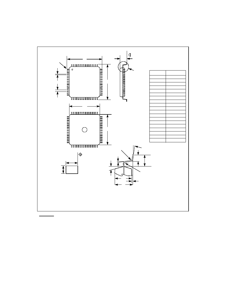
SMSC DS ≠ LAN83C183
113
Rev. 12/14/2000
5.6 MECHANICAL DRAWING
This section contains the mechanical drawing for the LAN83C183 64-pin LQFP
package.
Figure 5.22 64-Pin LQFP Mechanical Drawing
Important:
This drawing may not be the latest version.
D
E
Pin 1
e
See
Detail B
E1
b
D1
A
See
Detail A
Symbol
b
e
ccc
ddd
D
E
L
L1
R
R1
A
A1
A2
c
D1
E1
@
@1
@2
Dimensions
0.17 ≠ 0.27
0.50 Basic
Max. 0.08
Max. 0.08
11.85 ≠ 12.15
11.85 ≠ 12.15
0.45 ≠ 0.75
1.0 Ref
0.08 ≠ 0.20
Min. 0.08
Max. 1.60
0.05 ≠ 0.15
1.292 ≠ 1.508
0.09 ≠ 0.20
9.90 ≠ 10.10
9.90 ≠ 10.10
0∞ ≠ 7∞
Min. 0∞
12∞
ccc
c
b
ddd
Detail B
L
@2
@1
@
L1
Note:
1. All Dimensions are in millimeters.
1. Dimensions do not include mold flash. Maximum allowable
flash is 0.25.
1. All leads are coplanar to a tolerance of 0.08 (ccc). Bent
leads to a tolerance of 0.08 (ddd).
A2
A
R
Dimension Table
R1
Detail B
A1

SMSC DS ≠ LAN83C183
114
Rev. 12/14/2000